Technology
2nm semiconductor challenges: Exploring Rapidus' technological breakthroughs
Semiconductors: The key to the modern world and cutting edge of innovation
Semiconductors are the foundation of today's digital society, constantly evolving to deliver faster speeds and greater processing power. The key driver behind these advancements has been circuit miniaturization—shrinking transistor sizes to fit more onto a single chip. Now, the industry is entering the 2 nanometer (2nm) era, representing the most advanced generation yet.
What are process nodes and why is scaling important?
In semiconductor manufacturing, the term process node refers to the generation of fabrication technology, typically measured in nanometers. A smaller nm number indicates finer processing capabilities and the ability to draw narrower circuit lines. While these numbers used to directly reflect the physical gate length of transistors, modern structures have decoupled the node name from exact dimensions. Today, node names like 2nm are rough indicators of generational advancement, generally following a 0.7x scaling trend per generation. Node scaling has a significant impact on performance, integration, cost and power efficiency. Smaller transistors shorten electron travel distances, speeding up switching and boosting performance. Higher transistor density enables more functionality per chip, while increasing the number of chips per wafer reduces manufacturing costs. Additionally, reduced gate size lowers the required charge for switching, cutting down power consumption—a critical factor for battery-powered devices and data center energy efficiency.
Process scaling improves all aspects of semiconductor design: performance, functionality, cost and power efficiency. This is why companies worldwide have raced to develop smaller process nodes, in line with Moore's Law, advancing roughly every two years.
A history of scaling and the physical limits of miniaturization
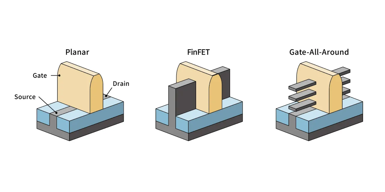
In 1965, Gordon Moore, who would later co-found Intel, proposed what became known as Moore's Law and outlined that every 18-24 months the number of components (like transistors) on an integrated circuit would double. This projection fueled decades of rapid advancement, driving better performance and lowering costs across electronics. However, as technology approached the 20nm node, traditional planar transistors encountered rising leakage currents and current flow when switched off, became a noticeable issue. Fin Field-Effect Transistors (FinFETs), introduced in the early 2010s, overcame this by shaping the channel into a vertical fin surrounded on three sides by the gate, effectively suppressing leakage.
Meanwhile, 193nm ArF excimer lasers used in photolithography struggled to form patterns below 10nm. This led to interim techniques like immersion lithography and multi-patterning before the eventual adoption of extreme ultraviolet (EUV) lithography, which enabled patterning at 7nm and below. Looking forward, further miniaturization will rely not only on transistor scaling but also on 3D integration, new materials, chiplets and novel transistor architectures for the post-Moore era.
The extreme engineering of 2nm: Why it matters
2nm semiconductors promise significant gains over earlier nodes, such as 7nm and 5nm. According to IBM's 2021 data on prototype 2nm chips, they can deliver 45% better performance or 75% lower power consumption compared to 7nm chips. While FinFETs enabled scaling through the 3nm generation, they encounter limitations with increasing leakage at even smaller dimensions. Enter gate-all-around (GAA) transistors. These use nanosheets or nanowires as the channel, completely surrounded by the gate, further improving control and suppressing leakage, enabling transistors to be made smaller while still achieving higher performance. IBM's prototype used a three-layer silicon nanosheet GAA structure, pushing beyond FinFETs in both performance and efficiency.
The 2nm node is especially important for AI and IoT. AI workloads demand extreme computing performance and energy efficiency, so semiconductors that can handle these requirements are essential. 2nm chips provide the needed processing power while remaining energy-efficient, ideal for AI servers and edge devices. For IoT, with its billions of small, often battery-powered devices, 2nm technology allows advanced AI to run locally without draining power. Still, 2nm presents formidable challenges. Variability and yield control become more difficult, and EUV lithography systems are incredibly expensive. Only a handful of companies worldwide can afford to produce at this level. However even with those challenges, 2nm is set to become the cornerstone of the next-generation digital infrastructure.
| Feature | 4nm | 3nm | 2nm |
|---|---|---|---|
| Introduction | 2021–2022 | 2022–2023 | ~2025 (planned mass production) |
| Transistor Type | FinFET | FinFET (some GAA) | GAA |
| Transistor Density | ~170M/mm² | ~250M/mm² | >300M/mm² |
| Performance | - | - | Up to 15–20% higher |
| Power Efficiency | ~10–15% better (vs. 5nm) | ~25% better (vs. 5nm) | Up to 30–40% better (vs. 3nm) |
| Mass Production Complexity | Medium–High (EUV early stage) | High (EUV + FinFET) | Very High (EUV + GAA) |
Rapidus' roadmap: Japan's leap into the 2nm frontier
In a fiercely competitive logic semiconductor market, global leaders like TSMC, Samsung and Intel are racing ahead.
Japan-based Rapidus, with backing from eight major Japanese corporations and support from Japan's Ministry of Economy, Trade and Industry (METI), was founded in 2022 with the goal of initiating 2nm mass production domestically by the late 2020s.
In partnership with IBM, Rapidus is advancing 2nm manufacturing. More than 150 engineers were dispatched to Albany, New York, in 2023 and 2024 to train in next-gen process technologies. Currently, about 80 of them have returned to Chitose and are working on tuning the processes for chip prototyping.
In April 2025, Rapidus started its pilot line at its Innovative Integration for Manufacturing (IIM-1) foundry in Chitose, Hokkaido, with sample production scheduled for later that year and mass production targeted for 2027.
Rapidus' new IIM-1 foundry represents a significant advancement over the traditional foundry model. The company is re-imagining how semiconductor factories should think, learn, adapt and optimize processes in real time through cutting-edge methods and technology.

Rapidus is also collaborating with California-based AI computing company Tenstorrent to co-develop AI processor IP for edge applications. Interest in Rapidus' 2nm technology is rising among global semiconductor leaders.
Rapidus is building a broad range of partnerships. In addition to IBM, its partners include nanoelectronics R&D hub imec and a wide range of equipment and materials manufacturers, which will have a presence alongside Rapidus in an advanced ecosystem centered in Hokkaido.
With deep technological capabilities and strong alliances, Rapidus is set to shine as a new Japanese force for the world's semiconductor elite.
Conclusion
Semiconductors continue to evolve as the foundation of the modern digital economy, with circuit miniaturization—process-node scaling—as a key enabler. The industry is now advancing into the 2nm era. IBM's 2nm prototype, released in 2021, demonstrated 45% performance gains or 75% power savings compared to 7nm chips. GAA transistor structures make this all possible by offering superior control and efficiency. In Japan, Rapidus is aiming to start mass production of 2nm chips by 2027. Through collaboration with IBM and others, the company is poised to become an influential player in next-gen semiconductor manufacturing, supporting the future of AI and IoT.
A type of transistor that is a three-dimensional improvement over the traditional planar transistor structure. Unlike planar transistors, the channel in a FinFET is formed as a fin-like shape protruding vertically from the substrate and the gate surrounds the channel from three sides—on the top and both sidewalls. It is named FinFET because the shape resembles a fish fin. FinFETs were developed to address the issue of leakage current that arises with miniaturization, and to achieve both improved performance and lower power consumption.
This is an advanced technology used in semiconductor manufacturing to transfer circuit
patterns onto silicon wafers. It is essential for producing extremely small semiconductors
using 2nm and 3nm processes.
The lithography (exposure) is a process similar to
developing photographs. A silicon wafer is coated with a light-sensitive material called
photoresist, and light is shined through a photomask that contains the circuit pattern.
The light passes through the mask and exposes the photoresist, transferring the pattern
onto the wafer. EUV lithography uses a special kind of light called extreme ultraviolet in
this process.
Traditional exposure technology, called Deep Ultraviolet (DUV), used
ultraviolet light with a wavelength of about 193nm. But to create even finer circuit
patterns, light with a shorter wavelength is required. EUV lithography makes it possible
to form ultra-fine patterns that were previously impossible, using extreme ultraviolet
light with a wavelength of just 13.5nms.
- #Semiconductor
- #Front-End
- #Transistor
- #GAA
- #Yield
Recommendation