Technology
What is EUV lithography? How this cutting-edge technology is powering Rapidus' next-gen semiconductor advancements
What is photolithography?
Photolithography is a technique adapted from photographic development to form circuit patterns on semiconductors. It is a foundational technology that supports the miniaturization of chips.
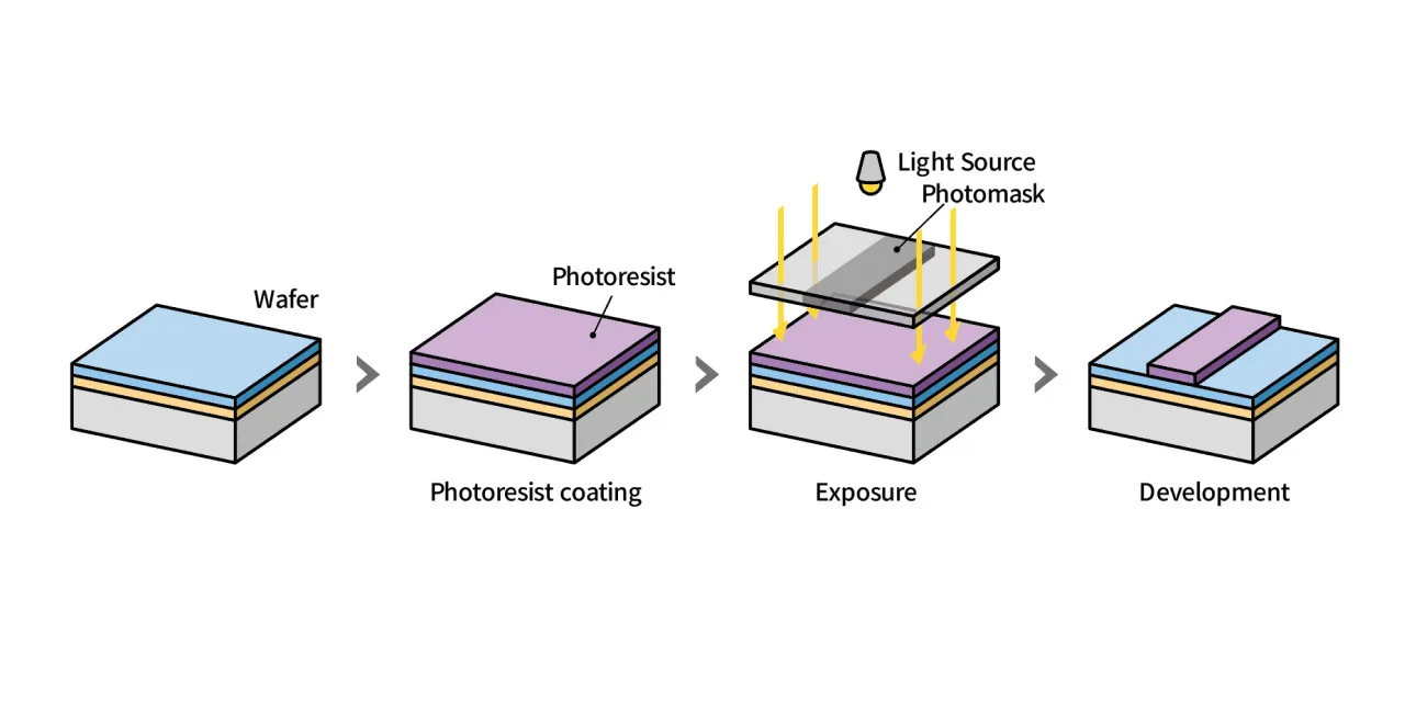
A photosensitive resin material called a photoresist is applied to a silicon wafer, and ultraviolet light is exposed through a photomask, a template with the circuit pattern. The exposed areas of the photoresist are dissolved with a developer, while the unexposed areas remain, transferring the pattern onto the wafer. In photographic terms, the photomask is similar to a film negative and the photoresist acts like photo paper.
As the semiconductor manufacturing process has advanced toward smaller nodes, higher resolution patterning has become critical. This requires improving the resolution of the light used, primarily by employing larger lenses and shortening the wavelength of the light source.
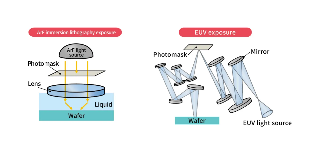
Shorter wavelengths have been key to this miniaturization. In the 1980s, g-line (436nm) light was used, followed by i-line (365nm) in the early 1990s, KrF excimer lasers (248nm) in the late 1990s and ArF excimer lasers (193nm) in the 2000s. To further enhance resolution, ArF immersion lithography was introduced in the mid-2000s. These advancements were accompanied by improvements in photoresists, lenses and other supporting technologies.
The rise of EUV lithography: A game-changer in photolithography
Even with ArF immersion and multi-patterning techniques—where patterns are exposed multiple times to achieve finer resolution—mass production below the 7nm node has faced major hurdles in complexity and cost.
This led to the emergence of extreme ultraviolet (EUV) lithography as the next-generation solution. EUV lithography uses light with an extremely short wavelength of 13.5nm, enabling the formation of patterns below 7nm—something not feasible with ArF lasers. Thanks to EUV lithography, continued miniaturization has progressed into the 5- and 3nm generations.
How EUV lithography works and technical challenges
The defining feature of EUV lithography is its use of 13.5nm wavelength light, which introduces a host of engineering challenges. Because EUV light does not naturally exist, it must be generated artificially within the lithography system.
The most widely adopted method is laser-produced plasma (LPP), in which a high-power CO₂ laser is fired at tiny liquid tin droplets, instantly creating a high-temperature plasma. The 13.5nm EUV light emitted during this process is used for exposure.
However, EUV light cannot pass through glass lenses or air. As a result, the entire exposure system operates in a vacuum and uses reflective optics instead of transmissive lenses. These optics consist of multi-layer mirrors coated with more than 40 alternating layers of molybdenum and silicon. However, these mirrors can only reflect about 68–70% of the light, meaning roughly 30% of the light is lost with each reflection.
Since the light must reflect off a dozen or more mirrors before reaching the wafer, only about 1% of the original light intensity actually hits the wafer. Although it's possible to transfer patterns with weak light by increasing exposure time, this drastically reduces throughput. To solve this, manufacturers have invested vast amounts of time and money into developing higher-output EUV light sources.
EUV lithography also requires reflective masks instead of conventional transmissive ones. Any defect or contamination in these masks directly translates into defects on the wafer. As such, defect-free and ultra-clean masks are essential. These masks are expensive, adding to the overall cost burden. Additionally, EUV-specific photoresists must be highly sensitive and transparent, with ongoing efforts to optimize sensitivity, resolution and line-edge roughness.
EUV light can also damage masks and mirror surfaces. If particles or debris adhere to the optics, they can cause fatal patterning defects. Therefore, protective coatings, in-situ cleaning technologies and preventive measures are critical for maintaining system performance.
Due to these complex requirements, EUV exposure systems are massive and highly intricate. They include tens of thousands of components, housed in large high-vacuum chambers filled with precision optical components. Often referred to as the most complex machines in the world, these systems are manufactured through a global supply chain involving thousands of specialized companies.
EUV mass production today and Rapidus' domestic milestone
Since the 1990s, EUV has been considered the ultimate next-generation lithography process, however, it took decades of development before entering mass production in 2018.
Today, the world's leading semiconductor manufacturers have adopted EUV for advanced chip production. The only company to have successfully commercialized EUV lithography at scale is ASML, based in the Netherlands. As a result, ASML currently holds 100% market share.
Each EUV scanner reportedly costs over $300 million. Despite the high price, EUV has become indispensable for manufacturing cutting-edge semiconductors, prompting major chipmakers to invest in these systems.
In December 2024, Rapidus installed Japan's first EUV scanner for mass production—the ASML TWINSCAN NXE:3800E—at its state-of-the-art Innovative Integration for Manufacturing (IIM-1) foundry in Chitose, Hokkaido.
Just three months later, on April 1, 2025, installation was completed, and the system was connected to a coater-developer track. Shortly after this, Rapidus successfully performed full-auto EUV pattern exposure and development, a major milestone toward volume production.
Rapidus has licensed 2nm process technology from IBM, which it is working closely with through joint development and personnel exchanges. The goal is to begin mass production of 2nm chips by 2027. The deployment of EUV technology is a key part of Rapidus' strategy for becoming a domestic pioneer in advanced semiconductor manufacturing.
Conclusion
EUV lithography is an essential technology for producing the most advanced semiconductors today. Using 13.5nm extreme ultraviolet light, it enables patterning at 7nm and below. Despite numerous challenges, the technology has matured into a practical and scalable solution.
Rapidus, committed to revitalizing Japan's semiconductor industry, has taken a major step by becoming the first company in Japan to install a production-ready EUV scanner. This move towards mass production of 2nm logic chips positions Rapidus as a critical player in returning Japan to the forefront of global semiconductor innovation.
A technique used to form extremely fine patterns that cannot be created with a single exposure. It involves multiple cycles of exposure and etching (or deposition). It was developed as a workaround to extend conventional lithography methods before EUV became viable.
A technique where a liquid, typically pure water, with a higher refractive index than air is placed between the projection lens and the wafer. This improves resolution and enables smaller circuit features than dry lithography.
- #Semiconductor
- #Front-End
- #Wafer
- #Single-Wafer Process
Recommendation