Technology
Why is Semiconductor Design So Hard? – A Behind-the-Scenes Look at Rapidus' High-Speed Chipmaking Process
What is Semiconductor Design?
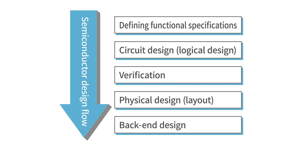
A Long Journey from Specifications to Back-End Design
Designing a semiconductor chip takes many careful steps. It starts with figuring out what the final product needs to achieve. Then, engineers create a circuit design (called logic design), check if it works correctly (verification), lay out the parts (physical design) and finally prepare it for back-end design.
First, the team writes down exactly what functions and performance the chip must achieve. Based on that, they design how the circuit should behave using something called register transfer level (RTL) design and logic synthesis. Second, they use simulation and verification tools to make sure the logic works as expected. In the physical design stage, they decide where to place tiny parts like transistors and how to connect them with wiring. The last stage is called back-end processing, which creates the final photomask data needed to make the chip. This part also considers timing, power use and how the chip will actually be built.
Each stage takes a lot of checking and fine-tuning. It requires deep knowledge and hard work to turn a chip design into something that can actually be manufactured.
EDA, IP Library, and PDKs: The Three Must-Have Tools for Faster and Better Chip Design
To design semiconductor chips faster and make sure they can actually be built, engineers rely on three powerful tools: electronic design automation (EDA), intellectual property (IP) libraries and process design kits (PDKs).
EDA tools automate many steps in chip design, from drawing the circuits to verification, laying out the parts and creating the final data. This saves time and helps avoid making design mistakes. IP libraries are collections of circuit parts that have already been tested and used before. Engineers can reuse them like blocks, which makes the job easier and more reliable. PDKs include special rules, simulation models and standard cell information optimized for the manufacturing process, serving as a bridge between the design part and the manufacturing part.
When these three tools are used together—EDA for automation, IP libraries for reusability and PDKs for buildability—they help engineers design much better chips, more quickly. That is why they are essential for creating today's most advanced semiconductors.
Why is Semiconductor Design So Hard?
The One-Billion-Transistor Era has Changed Everything
The latest chips inside smartphones and computers have become way more powerful over time, following a trend known as Moore's Law. Now, a single chip, just a few centimeters wide, can hold billions or even tens of billions of tiny transistors. As a result, designing these chips has become increasingly complicated. Engineers have to make sure every single transistor works correctly and accurately. That is a tough job, especially when designing logic and timing. It puts a heavy load on the designers.
In addition, today's chips need to be super powerful while using less energy. Designers also have to worry about various challenges, like heat, electricity leaks, and keeping power use low. Designing a chip now takes longer than ever, and it is getting more difficult to keep up productivity, and. This is why semiconductor design has become such a challenging field - one that needs advanced skills and smarter tools to stay ahead.
Designing Easy-to-Make Chips - DFM and OPC
Design for Manufacturing, or DFM, is a way of designing chips while thinking ahead about problems that might happen during manufacturing. The goal of this design method is to improve how many good chips you get, called yield, and how reliable they are. Today's chips are produced in incredibly small sizes, measured in nanometers, so it is hard to draw the tiny patterns perfectly on the wafer. Things like machine differences and the limits of light used in the process can cause defects, called "hotspots."
That is where Optical Proximity Correction (OPC), comes in. It adjusts the photomask data slightly ahead of time to make sure the printed pattern looks like what was intended.
But OPC cannot fix every issue, especially when the layout is really complicated or when equipment varies too much. So DFM takes a further step, which tries to avoid risky patterns during the design phase, fixing them before they cause problems later.
To make high-quality chips efficiently, engineers must now be aware of the manufacturing process right from the start of the design.
Rapidus' Big Idea: Making Design and Manufacturing Work Better Together
MFD and DMCO: From Easy to Build to Design-Friendly
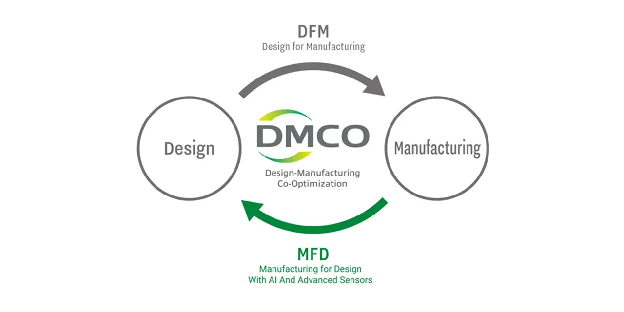
Designing chips has gotten more and more complex, so engineers are coming up with smarter ways to make the process more efficient. A new concept that Rapidus has pioneered is called Manufacturing for Design (MFD). This drives a strategy that shifts from designing easy-to-build chips to creating factories that make it easier to design advanced chips.
With MFD, factories use AI and sensors to collect lots of data while making chips. This data is then sent back to the design team as feedback. This enables designers to adjust their work using real data from the factory, which helps them build in more flexibility and avoid problems later.
Rapidus also introduced Design-Manufacturing Co-Optimization (DMCO), which combines MFD and DFM. DMCO brings design and manufacturing closer together, especially for next-generation chips like the 2-nanometer node size. By checking and adjusting how design and manufacturing affect each other again and again, Rapidus hopes to build better chips, improve success rates and lower costs at the same time.
Raads - AI System that Accelerates Chip Design Phase
Rapidus AI-Assisted Design Solutions (Raads) is a special tool made by Rapidus that uses AI and machine learning to help with chip design. It builds on the usual way of designing chips, called standard-cell design, but adds the power of AI to speed things up. With Raads, the time it takes to design a chip can be cut down a lot.
Raads helps with many parts of the process, from reading a design written in natural language to creating the final mask patterns used in manufacturing. This makes chip design both faster and more efficient.
Because of this speed, even very advanced chips, like 2-nanometer ones, can be designed in less time. In the end, Raads aims to give more designers the ability to work on advanced nodes and technology, helping to boost the entire semiconductor ecosystem.
Rapidus' Disruptive Business Model: RUMS
Rapidus' concept of Rapid and Unified Manufacturing Service (RUMS) refers to a bold new business model in which one organization handles everything from chip design to making the wafers and packaging the final product, all in one smooth process.
Usually, these steps are done by different companies. But Rapidus brings them all together under one roof. Using RUMS, Rapidus will be able to create and deliver the latest chips, including 2-nanometer ones and chiplets, faster than anyone else in the world.
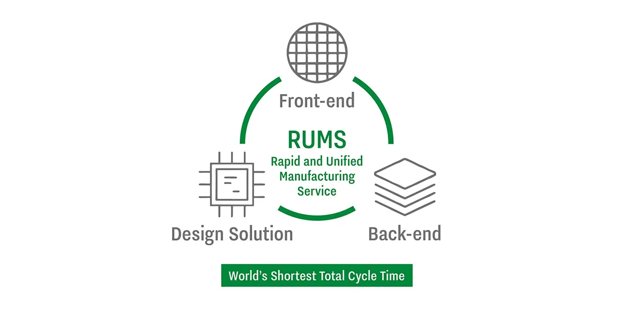
The concept behind RUMS is integrative co-creation. And, as the name Rapidus suggests, the goal is speed, making both the design and manufacturing processes as rapid as possible, from start to finish.
A PDK is a package of important files that chip designers need when designing semiconductor circuits. It contains information like how transistors behave, what rules to follow when designing the chip, and tools for simulating, laying out and checking the design. PDKs are usually provided by foundries to the companies that design chips.
A transistor is a tiny part in a chip that can make electrical signals stronger or turn
them on and off. Modern ICs use a type called Metal-Oxide-Semiconductor (MOS). It is made
of three layers: a metal gate, an insulating oxide layer, and a silicon base. It also has
three terminals: the gate, source and drain. When voltage is applied to the gate, it
creates an electric field across the oxide layer. This changes the way electricity flows
inside the chip. In an n-type MOS transistor, adding positive voltage to the gate forms a
path, or a channel, that lets electrons move from the source to the drain, which is how
current flows.
Most chips use a setup called CMOS, which uses both n-type (NMOS) and
p-type (PMOS) transistors together. Moore’s Law, which predicted that chips would keep
getting smaller and more powerful, was made possible because MOS transistors are simple
and easy to shrink.
- #Semiconductor
- #Design
- #Design Solution
Recommendation