People
Overcoming the challenge of 2nm development lies the path to a differentiated technology lead
On July 18, 2025, Rapidus unveiled its first wafer featuring a gate-all-around (GAA) transistor
fabricated using a 2 nanometer (nm) process. This milestone was reached just over three months
after transporting an extreme ultraviolet (EUV) lithography system in December 2024 by air from
the Netherlands.
By June 2025, the first production lot had been processed, and the
resulting GAA transistor wafer was showcased at a customer event in July. Rapidus attributes
this exceptionally rapid establishment of production capability to its defining manufacturing
strength.
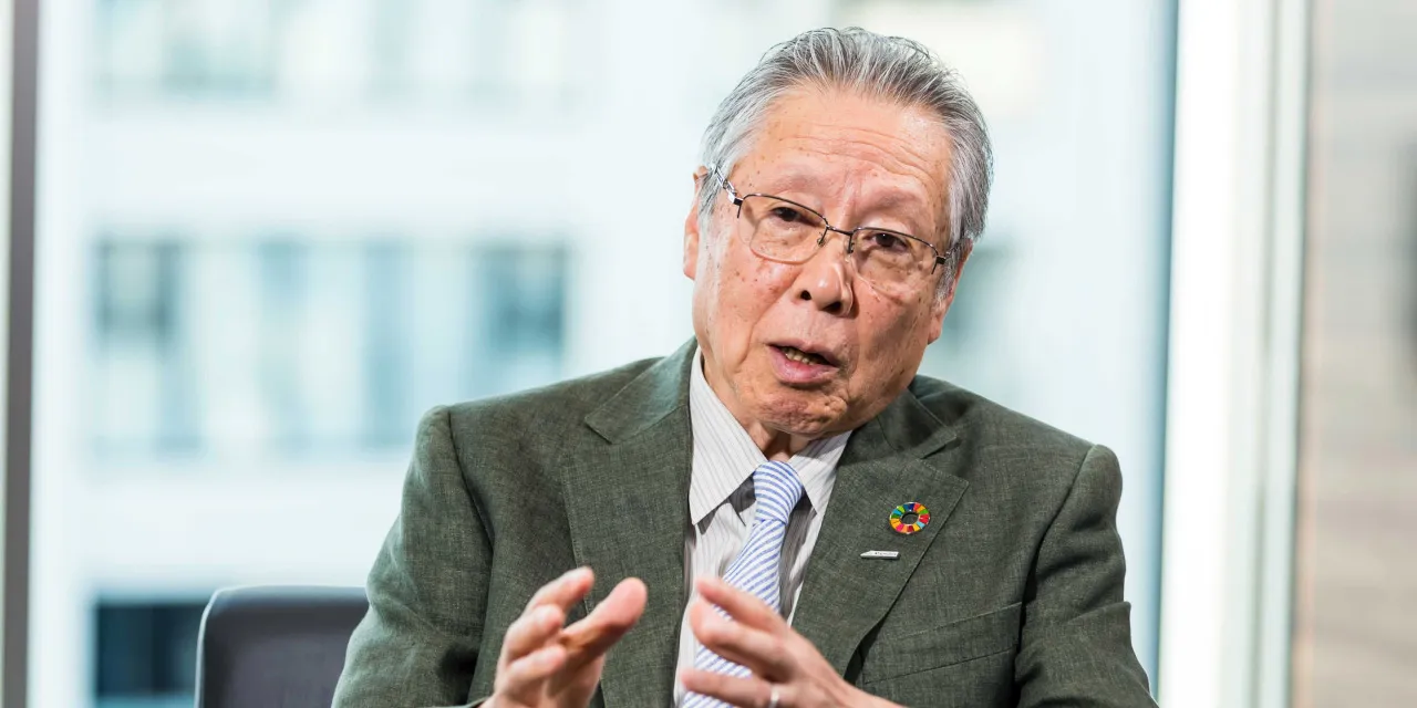
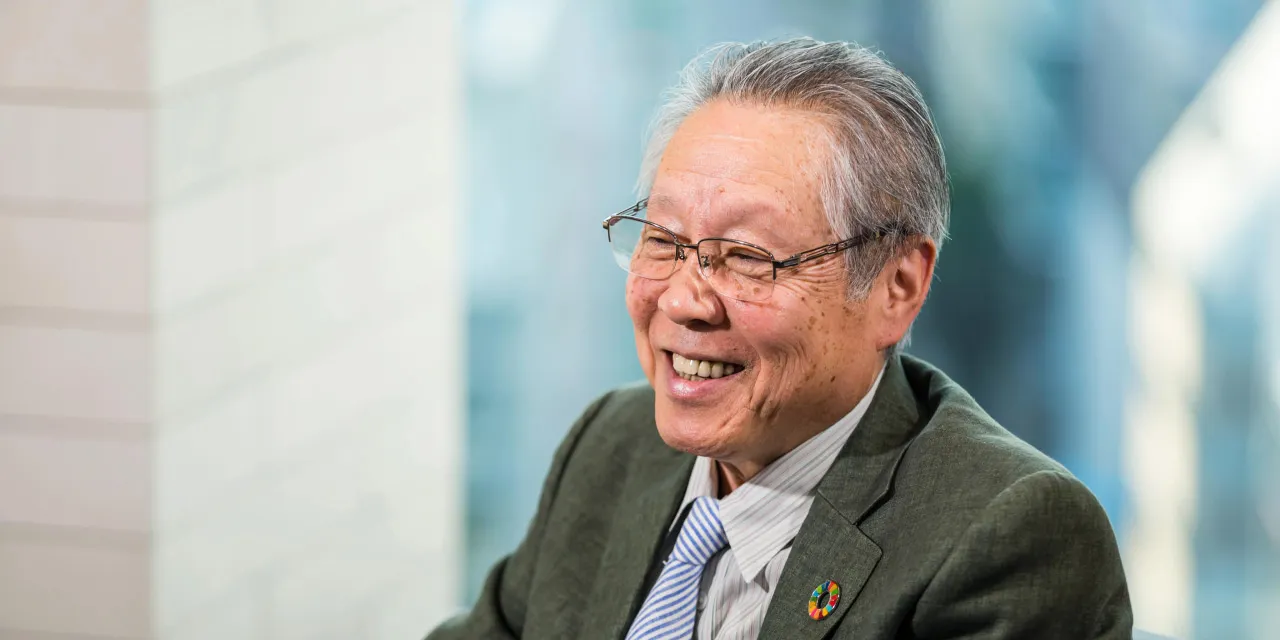
We spoke with Rapidus Chairman, Tetsurō Higashi, about the challenges and
milestones since the company’s founding in August 2022 through its latest achievement.
―― I vividly recall the panel discussion at SEMICON Japan in December 2020, discussed the revival of Japan's technological leadership. Just a year and a half later, Rapidus was established. Can you share the process leading up to the formation of Rapidus in August 2022?
In the summer of 2020, IBM approached me with a proposal to implement a 2nm process using GAA transistors in Japan. When I consulted Japanese semiconductor manufacturers, they plainly stated they could not pursue such an initiative—confirming that established Japanese firms could not take on cutting-edge logic. But launching a company alone was insufficient. Without access to advanced semiconductors, Japan faced a dangerous situation on an economic security crisis.
Launching a semiconductor business requires technology, people and capital. First, I consulted with Atsuyoshi Koike, then president of Western Digital Japan and a Toshiba partner in NAND flash production to assess the technical feasibility of GAA 2nm. Over the next year, I assembled a list of potential talent in Japan and globally. Although Japan was pursuing TSMC's establishment of a fab in the Kyushu area, their 22nm/12nm lines were not close to 2nm capability. Thus, in August 2022, we founded Rapidus.
At inception, we planned to collaborate with the Japan government—but to secure that support, we needed confirmation that system integrators were interested in 2nm technology. Between August and October, we visited major Japanese companies, resulting in eight of them investing in Rapidus. To move forward, we had to obtain an EUV tool—so in the summer of 2022, we met with the leadership at ASML and worked to establish a partnership that would bring their equipment to Japan. The public announcement followed in November.
―― As Rapidus approaches its third anniversary in August 2025, how do you feel about the company now?
We have remained on schedule at every major milestone. Following the groundbreaking ceremony in September 2023, construction of our Innovative Integration for Manufacturing (IIM-1) foundry commenced and progressed swiftly. By December 2024, equipment delivery began, and within three months more than 200 systems had been installed in our factory. 2025 milestones include demonstrating EUV patterning in April, processing of the first lot in June and in July at our first customer event, we announced operation of the 2nm GAA transistors on a prototype wafer. Going forward, we will refine these samples and begin phased customer evaluations.
While this sounds like strict adherence to our plan, what stands out is the extraordinary speed of our team. Typically, drawing patterns from EUV installation takes nearly six months—but we accomplished it in three. Employee count has grown from a dozen at founding to 800 full‐time employees and more than 1,000 temporary staff. We hire 30–40 people per month. These experienced engineers are highly motivated, enjoy their work immensely and expectations are high.
We sent approximately 150 engineers to IBM's site in Albany, New York, for two years of joint development and training on GAA. Half of them have returned to Chitose. We are now transferring the outcomes of the 2nm GAA research there. In three years, we have built a solid foundation. They return with confidence that they can stand alongside those who once worked with IBM—and that confidence is exactly what Rapidus needed.
―― The semiconductor landscape has changed dramatically—especially with the rise of generative AI. What has shifted?
AI has evolved rapidly into generative AI, driving demand for new semiconductors. Today's strongest demand is in AI data centers, but we are entering a new era of AI at the edge and in daily life. For example, AI applied in primary industries such as agriculture, fishing and dairy farming can improve productivity. I learned from a young dairy entrepreneur in Hokkaido who is passionate about applying AI to develop the local industry—that Hokkaido milk can now be found in high-end European ice cream. I believe the convergence of AI and Hokkaido can unlock new stages of growth.
Since the Meiji era, pioneers from mainland Japan helped develop Hokkaido. As Rapidus establishes our fab there, we're hoping it will spark a similar kind of catalytic development—not only for Rapidus but for the region. At Hokkaido University, student presentations often conclude with the statue of Dr. Clark, "Boys, be ambitious!"—I feel that spirit is still alive there. In the Silicon Valley, educational institutions grew around semiconductor companies, supported infrastructure and attracted global talent. Hokkaido's local government and communities are equally committed to building such an ecosystem. I have high hopes.
―― What role does Rapidus play in the future of Japan's semiconductor industry, and what are your aspirations for Japan semiconductors moving forward?
Semiconductors are critical from an economic and national security perspective, so the significance of a company like Rapidus continues to grow. Possessing advanced semiconductor capability brings clear geopolitical opportunities. Rapidus leapt over 16nm through 3nm FinFETs to directly pursue 2nm. Initially, many wondered whether such a leap was realistic, and there was hesitation about bypassing intermediate steps. I think of this situation through a pendulum model: at the highest point of the pendulum's speed is zero; at the lowest, its speed is greatest. We entered at that pivot point—when game-change speed is zero.
While developing 2nm as a startup is difficult, success yields business advantage. Going forward, semiconductors will increasingly shift from general purposes to domain-specific designs—both for performance and power efficiency. General-purpose CPUs include unnecessary functions that still consume power, whereas dedicated semiconductors deliver only required capabilities, reducing wasted energy.
We want to demonstrate, "Yes, Japan can." If Rapidus succeeds, it will inspire the next generation of innovators. New challenges inevitably bring adversity—but overcoming adversity produces differentiated technology. Embracing failure with courage brings fulfillment. Veteran engineers—who joined mid-career, possess deep knowledge of Japan's semiconductor legacy—and fuel the younger generation with energy. Our team continues to grow, and being in this environment now is an incredible opportunity.
Creating a culture where young people can learn from challenging experiences, apply those lessons and keep pushing forward is essential. Companies must show that risk-taking is welcome—this mindset is vital to shaping the culture we need.
- #Interview
- #Tetsuro Higashi
- #GAA
- #AI
Recommendation