People
Rapidus' 2nm pilot line starts operation "We Can Do It!" — Rapidus CTO Kazunari Ishimaru on the future of Japan's advanced semiconductors
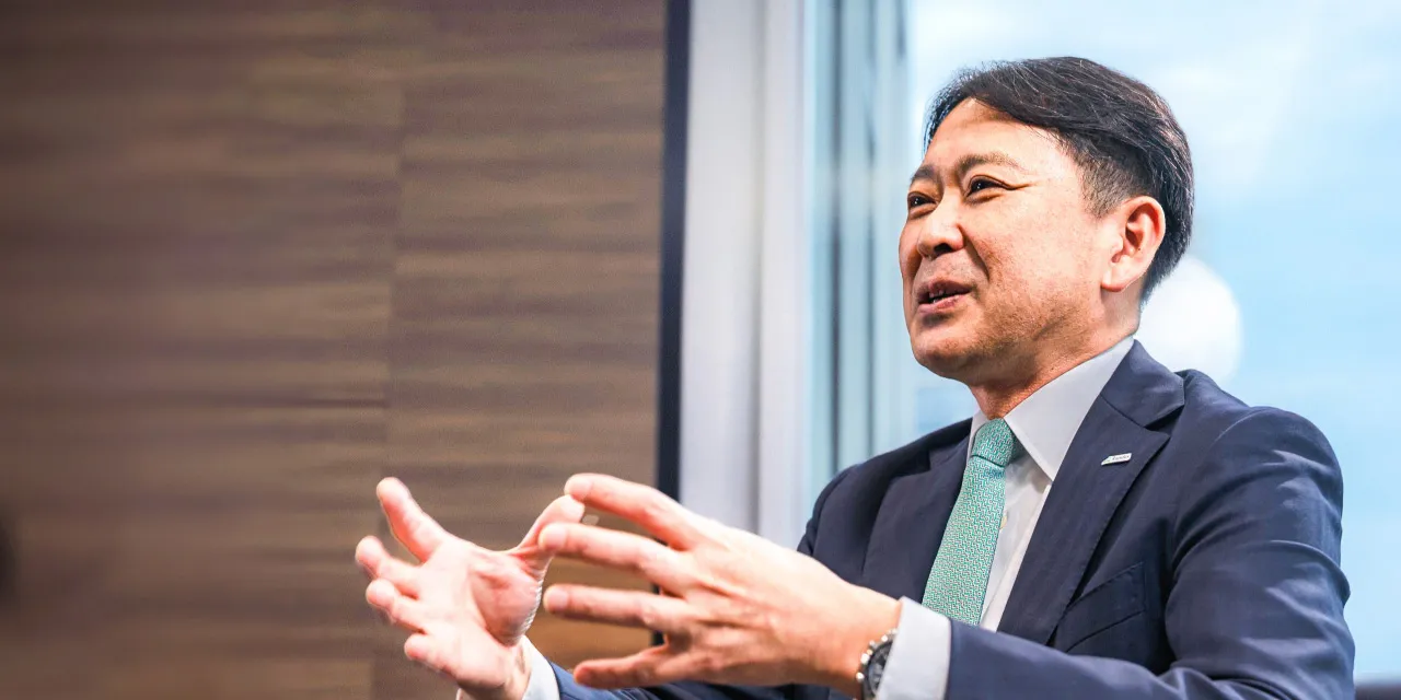
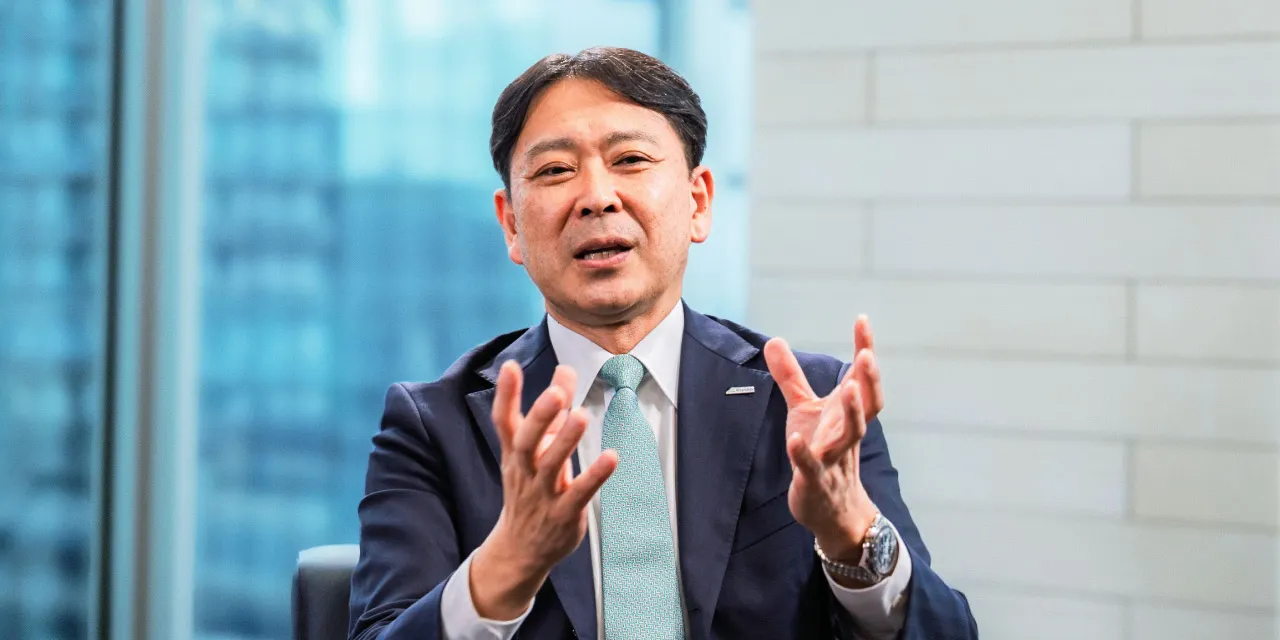
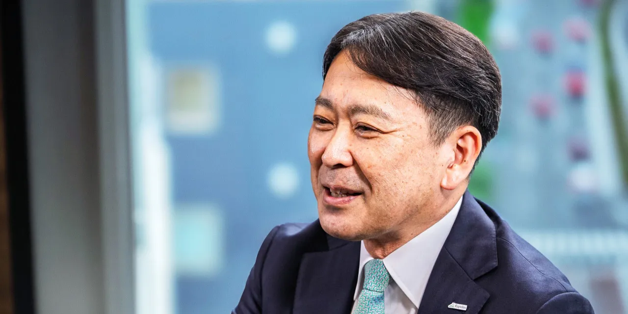
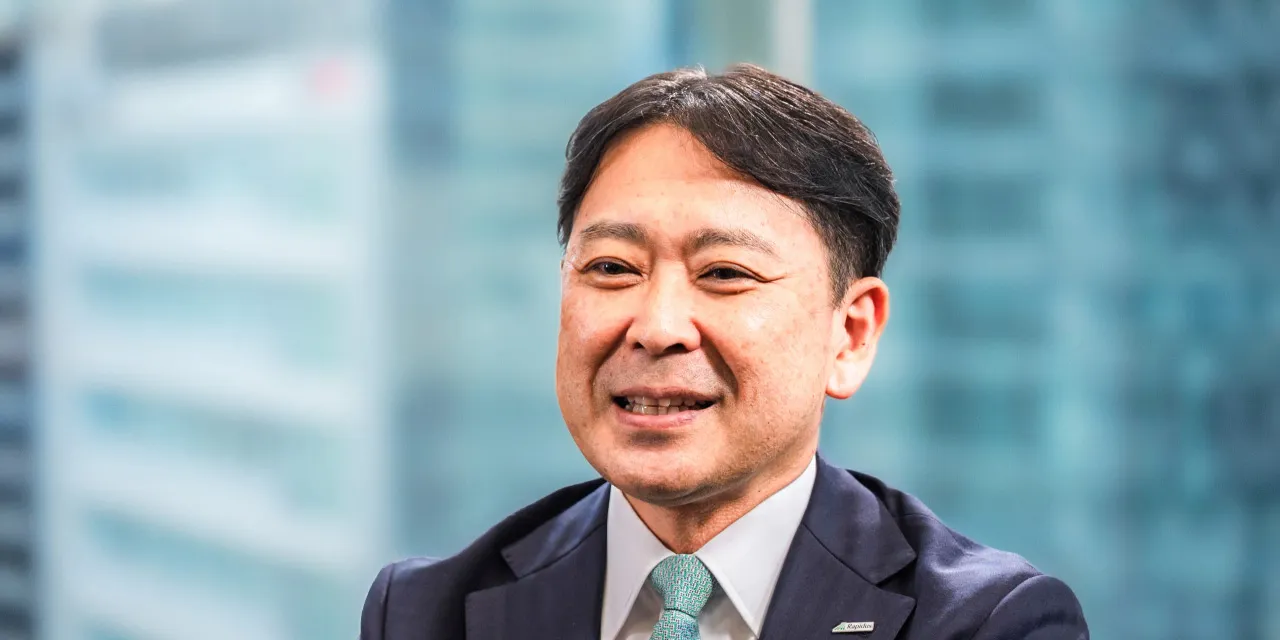
Kazunari Ishimaru
CTO
Key Points of This Interview
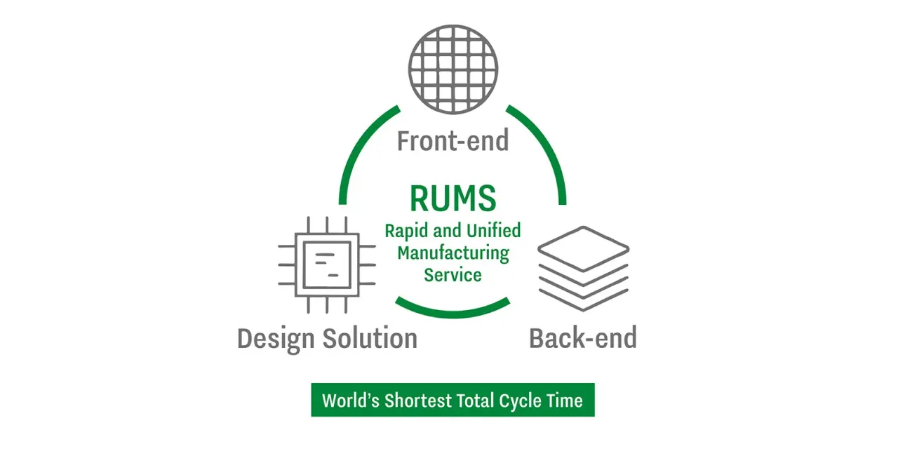
- Rapidus is building a next-generation foundry model through RUMS, integrating design, front-end and back-end processes.
- Engineers trained with IBM in Albany are now driving 2nm pilot production at IIM in Hokkaido.
- Through AI, Raads and vertical integration, Rapidus aims to dramatically shorten chip development time.
In April 2025, Kazunari Ishimaru was appointed chief technology officer (CTO) of Rapidus. In this interview, he unveils his technical strategy to revive advanced logic semiconductor manufacturing in Japan. He discusses key initiatives toward realizing a next-generation foundry model, including front-end/back-end integration under the Rapid and Unified Manufacturing Service (RUMS) concept *1, talent development systems and the development of the design support tool, Rapidus AI-Assisted Design Solution (Raads) *2.
CTO appointment and technical vision
―― You assumed the role of CTO at Rapidus in April 2025. Would you share your thoughts on your responsibilities as CTO and Rapidus' role going forward?
The CTO bears the heavy responsibility of overseeing all technical aspects. Personally, I feel strongly that I want to help bring advanced semiconductor manufacturing back to Japan through this role.
Rapidus is not merely a company that manufactures semiconductors. The manufacturing technologies we offer aim to enhance the quality of life for people. Using the power of technology to help realize a safer, more comfortable and happier society—is Rapidus' purpose and the driving force behind my work as CTO.
In the coming era, the demand for advanced logic semiconductors will continue to grow, driven by AI, data centers, autonomous driving and healthcare. In this context, restoring Japan's manufacturing prowess holds great significance.
Experience gained through IBM collaboration and motivation for joining Rapidus
―― How have you been involved with semiconductor technologies? And what led you to join Rapidus?
I joined Toshiba in 1988 and began my career developing high-speed SRAM and other memory technologies. Later, I worked on elemental technologies for logic devices and participated in advanced process R&D in the U.S. through a Toshiba-IBM collaboration.
Starting in 2006, I was involved in development projects for the 32nm, 28nm and 20nm nodes in collaboration with IBM. I spent about four and a half years immersed in state-of-the-art logic development at sites such as the TJ Watson Research Center, the East Fishkill fab and the Albany Nanotech Center in New York state.
Unfortunately, the 28nm process technology developed with IBM never made it to a domestic Toshiba fab, as Toshiba withdrew from cutting-edge logic manufacturing. However, the knowledge and networks I gained during that time are directly linked to where Rapidus stands today.
After returning to Japan, I worked on technology development for logic products and flash memory at Toshiba, then became deeply involved in next-generation memory R&D. During that time, I joined a private study group called the Mt. Fuji Project, organized by volunteers aiming to revive advanced semiconductor manufacturing in Japan. At first, I was skeptical, wondering, is this really possible?
But when I reunited with passionate members like Mr. Koike and reconnected with former IBM colleagues still holding key positions and actively engaging in discussions, my doubts turned into conviction: this time, transferring advanced logic production to a Japan foundry could truly—and finally—be achieved.
Initially, I joined Rapidus through a temporary position but soon felt that a true commitment was necessary. So, I left Toshiba and formally transferred to Rapidus to fully dedicate myself to the challenge.
"It Can Be Done"
―― What gave you the confidence that this time it really "can be done"?
First, many of the engineers I worked with at IBM are still active on the front lines. The fact that they understood both current challenges and advances in manufacturing, and had a well-thought-out scenario for success gave me strong confidence.

Second, from a technical standpoint, I had a realistic outlook on the structural complexity involved. The gate-all-around (GAA) structure used in the 2nm node is undoubtedly intricate, but based on my past experience in technology development, I could see that it was not physically impossible. With the right procedures, it could be realized.
Of course, I understood that turning a technology into something ready for mass production entails many technical hurdles. But I also believe that Japanese engineers involved in semiconductor manufacturing excel at persistent process optimization and fine-tuning. This capability translates into strong problem-solving power during ramp-up.
In short, both a compelling reason to do it and a solid technical foundation for achieving it came together, transforming any doubt into conviction.
CTO missions
―― As CTO, what are the key missions you are currently focused on?

I have outlined eight major themes, but the core pillars are: integration of front-end and back-end processes, formulation of a technology roadmap and advancement of human capital strategies.
Under the concept of RUMS, we aim to optimize what were traditionally separate domains—semiconductor design and wafer fabrication (front-end), and packaging (back-end)—into a unified, end-to-end process. We are advancing this initiative as a cross-organizational project with clearly defined company-wide collaboration and accountability structures. Although this approach is rare in the industry, we see it as one of Rapidus' core technologies.
In addition, we are working urgently to establish a technological roadmap that looks five to ten years ahead. We are building a framework that starts with clearly defined customer values and works backward to determine the technologies required to deliver that value.
Most important of all, however, is people. We already have many highly capable individuals from diverse backgrounds, but we also need to proactively involve the next generation. To that end, we have established a Technology Strategy Office under my direct supervision, which includes a Talent Development Working Group. This group, in collaboration with engineers experienced in education and our HR department, is working to define the ideal engineer profile for Rapidus and to design recruitment and training programs based on that profile.
We are also focusing on re-skilling to create systems that draw out the full potential of our existing workforce. People are not costs, they are assets. As CTO, I see it as my mission to move forward both technology and talent strategies in tandem.
Manufacturing innovation through RUMS and vertical integration
―― The RUMS concept promoted by Rapidus clearly differentiates it from conventional foundry business models. What are its goals and technical challenges?
RUMS stands for Rapid and Unified Manufacturing Service, a production model that provides integrated support from design through front-end and back-end manufacturing.
Traditionally, the foundry business has been built on horizontal specialization, where design, manufacturing and packaging are handled by separate companies. However, this often leads to unclear accountability when issues arise and results in significant time and cost losses.
To address this, Rapidus has envisioned a vertically integrated manufacturing support model, seamlessly connecting design support, wafer fabrication and packaging.
A key innovation is the integration of front-end and back-end processes. By consolidating both under one roof, we aim to dramatically improve the speed and precision of process optimization.
This unified structure will be a major advantage when dealing with multi-chip architectures, such as chiplets, which are expected to become mainstream in the near future.
Steady progress at the IIM pilot line in Chitose
―― Rapidus is steadily preparing for mass production at its Innovative Integration for Manufacturing (IIM-1) foundry in Chitose, Hokkaido. What is the current status of the pilot line?
Before launching the pilot line, approximately 150 engineers from Japan were dispatched to IBM's Albany, New York facilities to acquire knowledge for process startup. Currently, about 80 of them have returned to Chitose and are working on tuning the processes for chip prototyping.
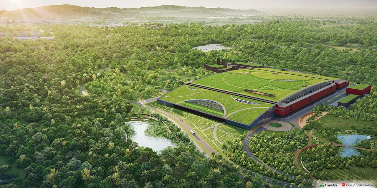
As of April 2025, more than 200 pieces of equipment were installed in Chitose, enabling the basic processes—meaning we can now physically form semiconductors. These steps were then connected into a full manufacturing flow spanning hundreds of processes. We confirmed whether these would actually yield functional chips and completed the acquisition of electrical characteristics of transistors in July 2025.
Right now, we're focused on further improving device characteristics and preparing for volume production.
Outlook on cutting production time in half
―― One of the core values RUMS promises is shortened manufacturing time. How much do you expect to reduce fabrication time in the front-end process?
Our goal is to complete wafer fabrication in less than half the conventional time compared to the traditional foundry. The keys to this are the single-wafer processing model and an AI-powered grid transport system.
Unlike batch processing—which handles multiple wafers at once under uniform conditions—single-wafer processing allows each wafer to be treated under its own optimized conditions. This dramatically improves both the accuracy and flexibility of process control.
Meanwhile, our AI-controlled grid transport system minimizes wait times and travel between tools, significantly reducing what we call non-processing time. This reduction, in turn, has a huge impact on shortening the overall manufacturing cycle.
We've also built a simulator that replicates the manufacturing line in a virtual environment with high precision. After running simulations under various conditions, we've been able to consistently produce wafers in under two months, so we're confident that our timeline is achievable.
Accelerating back-end processes
―― How do you plan to shorten the production time in the back-end process?
Compared to the front-end, automation in the back-end process has been slower to progress. Therefore, our first priority is to ensure thorough automation in this area.
Additionally, in chiplet architectures, a substrate is required for mounting the chips. In general, substrates are manufactured only after the chips are completed. However, with our vertically integrated production model that spans both front-end and back-end processes, we adopted a new concept: to start substrate manufacturing in parallel with chip fabrication.
By producing in parallel, we estimate that the back-end process time can be reduced by about half. Combined with AI-controlled material transport, and the fact that we are building a brand-new factory, we're able to incorporate such new concepts from the outset—achieving innovations that would be difficult to replicate in existing facilities.
DMCO and Raads: Enhancing design support
―― RUMS isn't just about manufacturing—it also includes design support. Would you explain your efforts in this area?
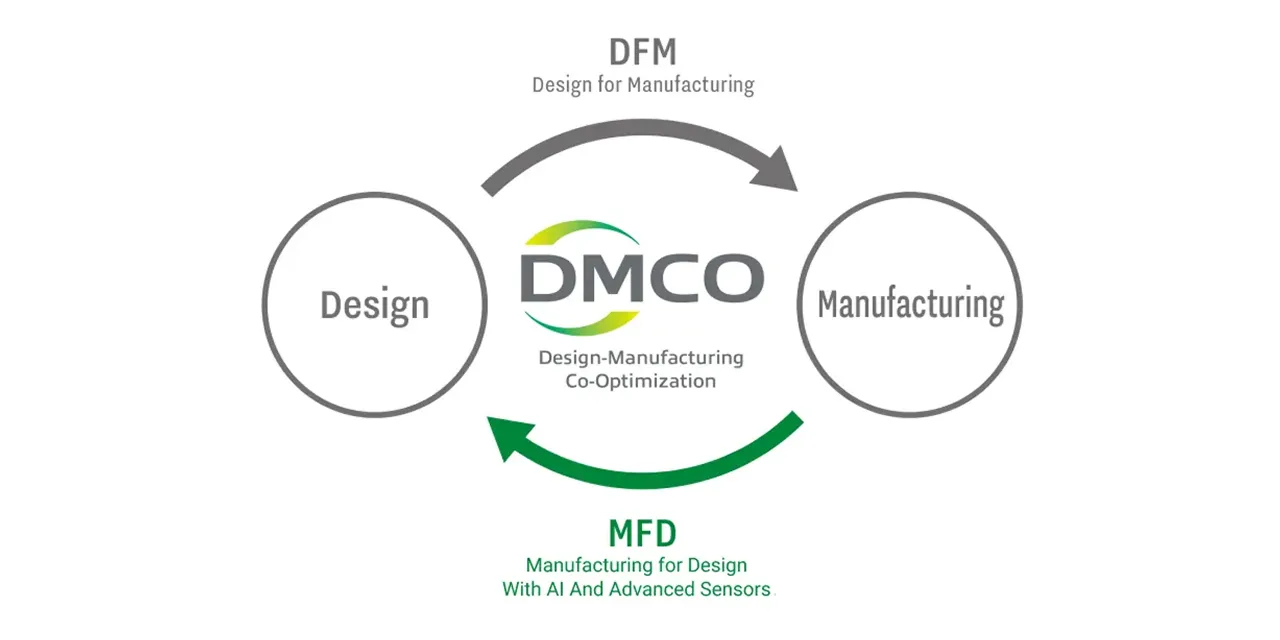
For RUMS to work, we need to strengthen not only manufacturing but also design support and design verification. We've already begun collaborating with EDA tool vendors, especially under the concept of Design-Manufacturing Co-Optimization (DMCO).
DMCO leverages large volumes of process data generated during manufacturing to feed insights back into the early stages of design. This reduces unnecessary design margins and helps maximize chip performance.
In terms of design support, we're also developing our own suite of tools called Rapidus AI-Assisted Design Solutions (Raads), developed to help designers create chips more easily and accurately.
One tool, Raads Predictor, allows for performance estimation even before the official Process Design Kit is delivered. Another, Raads Optimizer, suggests optimal combinations of circuit blocks, drastically improving design efficiency. We're also working on future tools like Raads Generator, which would automatically generate circuit designs based on functional requirements.
Integration with EDA tools
―― Is Raads designed to integrate with EDA tools?
Yes. Ultimately, design verification needs to be done using the high-precision tools provided by EDA vendors. However, Raads is most effective during the exploratory and conceptual design phase, when designers are still testing ideas.
Raads is envisioned as a free tool, intended to lower the barriers to design and enable more customers to work with advanced semiconductors. That's one of our core desires.
Broadening our network of design partners
―― It seems like Rapidus is expanding its network of partners in the design domain, including EDA tool vendors.
Yes, we are currently collaborating with multiple EDA vendors, IP providers and design solution companies, and we plan to announce further partnerships soon. Current partnerships include Cadence, Quest Global, Siemens EDA and Synopsys, to name a few.
What's most important is that Rapidus is not merely a contract manufacturing company—we aim to serve as a technical hub connecting the entire chain, from design to manufacturing and packaging.
Although we are less than three years old as a company, our ecosystem is steadily growing, thanks to the support of many partners who resonate with the vision behind the RUMS concept. Together, we are building genuinely meaningful collaborations.
A vision for people and society as CTO
―― Lastly, could you share your personal aspirations as CTO and what kind of future Rapidus aims to achieve?
Being CTO is a highly demanding role that oversees all technical domains. But for me, it's not just about managing technology—it's about thinking deeply about what kinds of technologies we should deliver to society to improve people's lives.
Semiconductors have become essential infrastructure. Therefore, the technologies we develop must contribute to a safer, more comfortable and more sustainable society. That's the kind of company we want Rapidus to be—a company that supports the future through the power of technology.
To achieve this, it's essential to work alongside outstanding talent and diverse partners. Ultimately, we want to build a team and a workplace that makes people think, "I want to work for that company," or "At Rapidus, I can realize my dreams."
We aim to be a proud community of engineers, committed to innovation and societal impact.
- *1. RUMS (Rapid and Unified Manufacturing Service): A new semiconductor manufacturing service model proposed by Rapidus. It provides integrated support from design to manufacturing and packaging, aiming to achieve the world's fastest cycle time.
- *2. Raads (Rapidus AI-Assisted Design Solution): A semiconductor design support service utilizing AI and machine learning (ML), designed to significantly shorten the design cycle time and reduce costs.
Related Links
- Rapidus https://www.rapidus.inc/en/
- Business and Technologies https://www.rapidus.inc/en/business/
- R&D and Manufacturing Base, "IIM" https://www.rapidus.inc/en/iim/
- #Kazunari Ishimaru
- #Interview
- #CTO
- #RUMS
- #DMCO
Recommendation