Technology
What are Chiplets? - The Key Technology Behind Next-Gen Semiconductor Manufacturing
With the rising demand for next-generation semiconductors, engineers are facing new technical challenges that traditional manufacturing methods can no longer address.
Is Moore's Law Reaching Its Limit? Current Challenges and Solutions
In 1965, Intel co-founder Gordon Moore proposed an idea called "Moore's Law," which has driven improvements in integrated circuit (IC) performance and cost reduction for over half a century. It became the foundation for modern digital technologies. This idea states that the number of transistors on a semiconductor chip would double roughly every two years.
For a long time, technological development has progressed in line with this law. But things have started to change. Shrinking chip circuits has become much more difficult recently, with line widths now reaching just a few nanometers (nm). Engineers are facing physical limits, more complex manufacturing steps and rising costs. Smaller circuits also mean lower yields, making it harder to produce a large number of usable chips. On top of that, building and running semiconductor foundries require huge amounts of money and expert knowledge. For these reasons, many now believe that Moore's Law cannot continue in the same way.
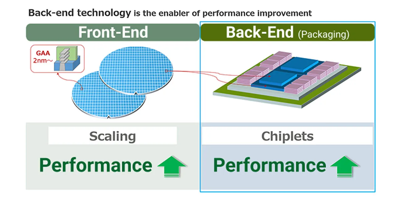
The end of Moore's Law has led to a new advancement: chiplets.
How Chiplets are Changing Semiconductor Design
A chiplet is a small piece of a chip (die) that performs a specific function, originally part of a single large chip. With chiplet integration, multiple chiplets are combined into a single package, where they work as a complete system.
In the past, all chip functions had to be built onto a single wafer. This meant that if even one part of a chip was defective, the entire chip had to be discarded. But with chiplet integration, only good chips - known as Known Good Die (KGD) - are used, which greatly improves manufacturing yields and efficiency.
Mixing and Matching: Heterogeneous Integration
Heterogeneous integration is a collective process that allows different dies, made with different processes and serving different functions, to be combined into a single chip package. Chiplet integration is especially effective for mixing and combining different types of circuits. For example, high-performance computing parts can be made using the latest semiconductor processes, while memory and analog parts can be produced using older, more cost-effective technologies. This balance helps improve performance while keeping costs low.
The automotive industry is particularly interested in this approach. Some major automakers are already using this technology in developing systems-on-chips (SoCs) for future vehicles, with plans to roll them out in production cars after 2030. One major advantage of chiplets is that they allow manufacturers to boost the performance and functionality of automotive semiconductors, improving AI computing and graphics capabilities more efficiently, while also increasing production yields.
Some automotive components need to meet strict safety standards. These are called functional safety components and usually use older, proven semiconductors. But modern systems like advanced driver-assistance systems (ADAS) and software-defined vehicles (SDVs) need much more powerful chips. This is where the chiplet technology comes in. With chiplets, manufacturers can create custom SoCs tailored to each automaker's needs faster by combining microcomputers for functional safety components, high-capacity memory, and powerful AI processors for self-driving.
These benefits are not limited to automotive applications. The chiplet technology is also spreading to other fields like AI and telecommunications, driving innovation across many industries. Chiplets are quickly becoming popular as a key technology for the future of the semiconductor industry.
Interposer: Integrating Multiple Chips into One
Chiplet integration depends on a technology that connects multiple chips in a way that is both compact and high-speed. The interposer is the key component that makes this possible. An interposer is a middle layer, usually made of silicon, that sits beneath the chiplets and connects them like a circuit board, helping the chiplets communicate with each other. The better the interposer, the more chiplets can fit closely together, and the faster they can exchange electrical signals.
Advanced chiplet integration technology also plays an important role in delivering power efficiently. Adding many tiny metal connection points between chips can provide enough paths for both electricity and data to flow, even in tight spaces. This allows for high-speed data transmission while making the most of the limited space inside the chip package.
Taking Chiplets to the Next Level with 3D Integration
Today, the mainstream method of chiplet integration is 2.5D integration, which places multiple dies into a single package. But the next big step is 3D integration, which is a technique that stacks chips vertically on top of each other. In a 2.5D structure, the dies are arranged side by side on an interposer to achieve high-density connections. In contrast, 3D integration stacks the chips vertically using a technology called through-silicon via (TSV), which allows even greater integration.
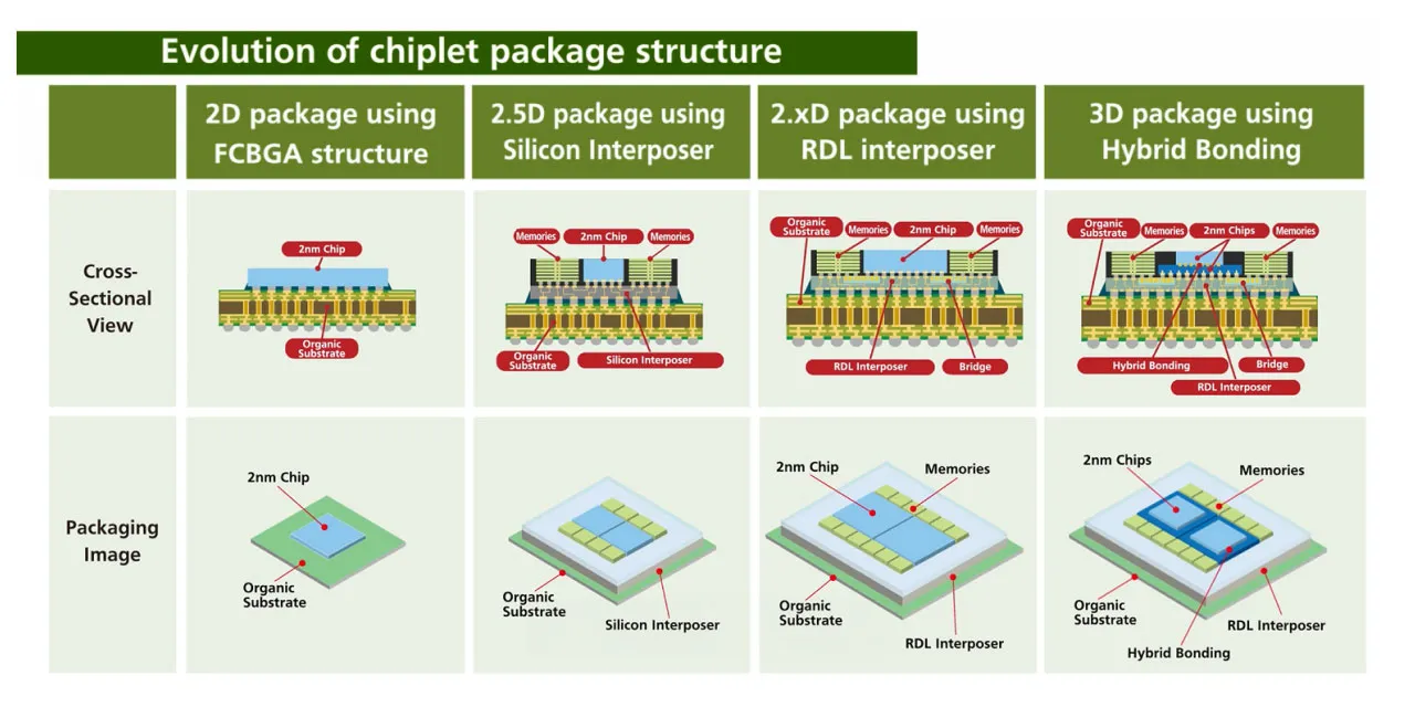
By combining the flexible design of chiplets, where different functions and circuit types are separated, with 3D integration, engineers can build faster, smaller and more energy-efficient semiconductors. Stacking memory and processing units directly on top of each other allows for high-speed access to large amounts of data, which is great for the fast execution of AI and other high-performance processes.
On the other hand, stacking chips vertically also presents new challenges. Heat tends to build up more easily, so thermal management and maintaining high manufacturing yields becomes more difficult. To overcome these issues, researchers around the world are working on new approaches for advanced packaging technologies to better address thermal challenges. But this is not slowing innovation. The combination of chiplets and 3D integration is now seen as a game-changing innovation that could take the torch from Moore's Law and lead the next era of semiconductor advancement.
How Rapidus is Advancing Chiplet Technology
Rapidus is working on advanced semiconductor technology for the 2nm generation as part of a government-backed project by the New Energy and Industrial Technology Development Organization (NEDO). As part of this effort, the company is also developing cutting-edge chip packaging that makes use of chiplet technology. Traditional silicon interposers, which connect chiplets, can become expensive when made larger. To solve this, Rapidus is turning to large-panel manufacturing using new materials like organic redistribution layer (RDL) interposers and glass carriers, which enables manufacturing large interposers more efficiently.
Unlike round silicon wafers, large square panels allow for cutting more chip substrates with less waste. This leads to higher yields and lower costs.
Glass carriers offer special advantages: they are flat, provide great insulation and manage heat expansion more effectively. They can even reduce signal loss in high-frequency circuits. When combined with the flexibility and performance of chiplets, glass carriers may lead to even more powerful and compact semiconductor systems. Rapidus is actively promoting research and development to overcome technical challenges, such as handling large panels and securing reliability.
By combining chiplets with new materials and manufacturing techniques, Rapidus aims to build high-performance and multifunctional semiconductors that go beyond Moore's Law, bringing new value to the global semiconductor industry.
TSV is a technology that creates tiny openings in a silicon chip and fills them with conductive material to make vertical connections. It lets stacked chips send electrical signals to each other quickly and efficiently.
- #Semiconductor
- #Back-End
- #Chiplet
- #Package
Recommendation