Technology
How Semiconductor Transistors Work: The On/Off Switches Powering Our Digital Society
Our digital society operates entirely on combinations of extremely simple information: 0 and 1. These numbers are physically generated by semiconductor devices called transistors, which form the core of modern electronic equipment.
Transistors function much like light switches in a room, allowing electric current to flow (on) or blocking it (off). By rapidly switching between these two states, transistors represent digital information as 0s and 1s. When countless transistors operate in coordination, computers are able to perform massive calculations and store vast amounts of data.
This article explores how transistors—simple electronic switches at their core—have evolved dramatically over time to become the foundation of today's digital society, highlighting both their history and the latest technological developments.

Basic Principles of Transistors
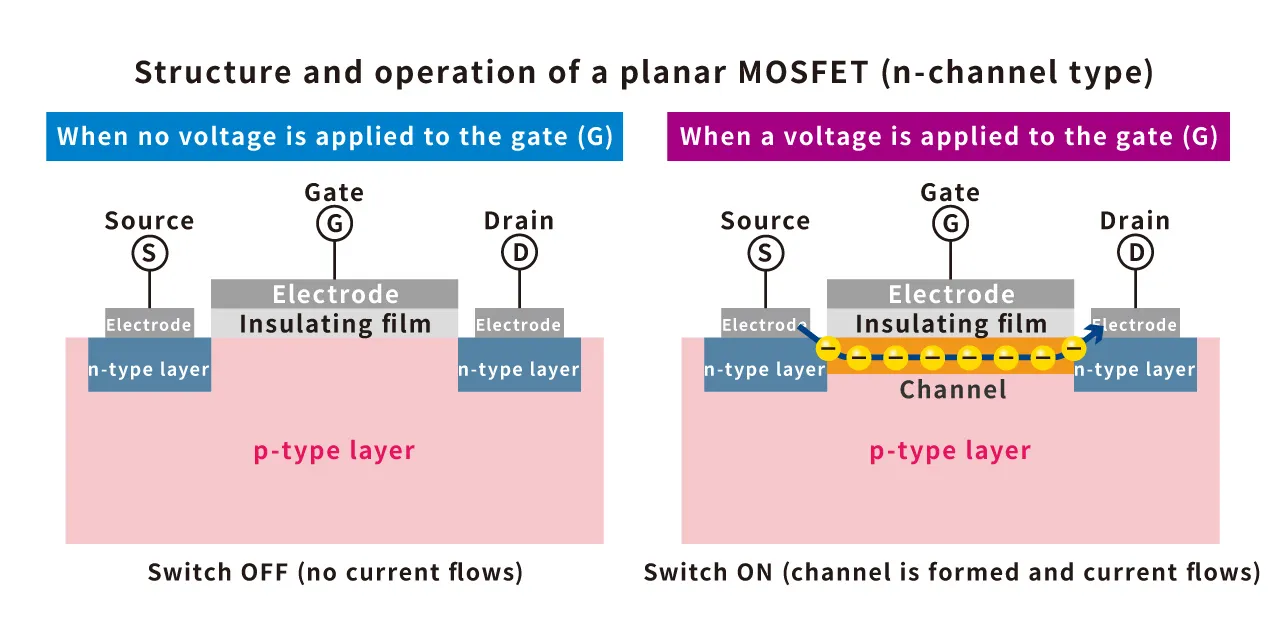
A transistor is a high-speed switch controlled by electrical signals. Inside the device is a control terminal called the gate. When a voltage is applied to the gate, it opens or closes a current path known as the channel.
When the applied voltage exceeds a certain threshold, called threshold voltage, the channel becomes conductive (on) and current flows. When no voltage is applied, the channel is blocked (off) and current does not flow. These on/off states are treated as digital information—0 and 1.
Such switching can also be achieved mechanically. However, transistor switching is electronic rather than mechanical, allowing it to operate at extremely high speeds. By controlling enormous amounts of 0s and 1s, collections of transistors can represent and process information such as numbers, text, images and video as digital data.
Even the photos and videos displayed on a smartphone screen are, internally, represented by hundreds of millions to billions of transistors, each taking either a 0 or 1 state. As the smallest functional unit of the digital world, transistors are indispensable elements underpinning all modern electronic devices.
The Invention and Evolution of Transistors
The Invention of the Transistor
Transistors are widely regarded as one of the greatest inventions of the 20th century. They were invented in 1947 at Bell Laboratories by John Bardeen, Walter Brattain and William Shockley.
At the time, electronic devices relied primarily on vacuum tubes, which were large and consumed significant power. A smaller, more energy-efficient alternative was urgently needed. This led to the development of the early point-contact transistor, a precursor to modern bipolar transistors that paved the way for miniaturization and reduced power consumption in electronic circuits.
For their research on semiconductors and the discovery of the transistor effect, the three inventors were awarded the Nobel Prize in Physics in 1956.

MOS Transistors
Following their invention, transistors continued to evolve. A major turning point came in the 1960s with the development of metal–oxide–semiconductor (MOS) transistors. As the name suggests, these devices consist of a three-layer structure: metal, oxide and semiconductor.
Compared with bipolar transistors, MOS transistors offer faster switching and significantly lower power consumption. As a result, most modern semiconductor circuits are based on MOS technology, forming the foundation of devices ranging from smartphones to supercomputers.
Why Make Transistors Smaller?
Since their invention, the primary driver of transistor performance improvement has been miniaturization—reducing the size of each switch. The main reasons for this are as follows:
Higher Performance
As transistors shrink, the distance electrons must travel inside the semiconductor becomes shorter, increasing on/off switching speed. This accelerates signal processing and computation, dramatically boosting a chip's overall performance.
In addition, smaller transistors allow more devices to be integrated into the same chip area, further enhancing computational capability.
Improved Energy Efficiency
Miniaturization reduces the amount of charge required for switching, lowering power consumption. Shorter current paths also reduce energy loss and heat generation.
Modern smartphone chips are manufactured using process technologies measured in just a few nanometers. With each new generation, power efficiency typically improves by around 20–30%, contributing to longer battery life. These advances also play a crucial role in reducing power costs in large-scale data centers.
Cost Reduction
When transistors become smaller, chips can be made more compact while maintaining the same performance. Smaller chips allow more units to be produced from a single silicon wafer, reducing cost per chip.
Driven by the combined demand for higher performance, greater energy efficiency and lower costs, the semiconductor industry has pursued miniaturization in accordance with Moore's Law, which predicts that transistor density roughly doubles every two years. This steady progression has supported the advancement of modern semiconductor technology.
The Limits of Planar Transistors
For many years, simply making transistors smaller was the main approach driving the semiconductor industry. However, this strategy eventually encountered physical limits.
In conventional planar MOS transistors, leakage current in the off state increases rapidly once gate lengths approach around 20nm. This leakage leads to power loss and can cause malfunctions. As leakage current grows, power continues to be consumed even when the switch is off, and digital circuits may fail to correctly recognize a 0, resulting in unintended operation.
These challenges became critical around process nodes with gate lengths of approximately 22nm, revealing the limitations of planar transistor structures.
Why Transistors Became Three-Dimensional
To overcome the limitations of planar transistors, engineers reexamined transistor structures themselves. By adopting three-dimensional designs, both higher performance and lower power consumption were achieved.
FinFET: A Key Breakthrough
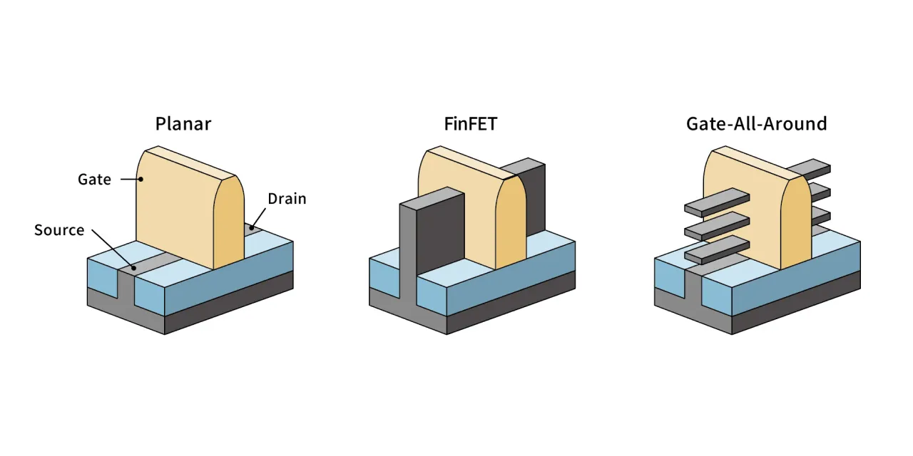
Commercialized in the early 2010s, fin field-effect transistors (FinFETs) feature channels that rise vertically like the dorsal fins of a fish. The gate surrounds the channel from three sides—top and both sidewalls—forming a tri-gate structure.
This design significantly strengthens electrostatic control, greatly reducing leakage current. At the same time, it allows higher on-state current and faster switching. FinFETs are still used in mainstream 5nm and 3nm process technologies, supporting the performance of CPUs and GPUs in smartphones and PCs.
Evolution to GAA Structures
Even FinFETs approach their limits at around the 3 nm generation. To address this, the next-generation Gate-All-Around (GAA) structure was developed. In GAA transistors, the channel is formed as nanosheets or nanowires, and the gate completely surrounds it from all directions.
This maximizes current control and minimizes leakage. In 2021, IBM announced the world's first 2nm prototype chip using GAA transistors with stacked silicon nanosheets, demonstrating higher performance and substantial power savings compared with same-generation FinFETs.
GAA transistors are expected to be introduced at scale in future cutting-edge nodes such as the 2nm generation, becoming a core technology for AI processors and next-generation CPUs. Compared with 7nm technology, 2nm chips are reported to offer up to 45% higher performance or 75% lower power consumption—advances made possible by GAA transistors.
Rapidus' Challenge in Realizing GAA Technology
Rapidus is working to realize next-generation semiconductors based on GAA structures. For the 2nm process generation Rapidus is targeting, adopting GAA technology instead of FinFETs is essential.
Mass-producing transistors at such advanced nodes requires highly sophisticated process technologies, including the precise stacking of silicon nanosheets and atomic-level etching to surround them with gate electrodes. To establish this technological foundation, Rapidus is actively collaborating with partners such as IBM and imec, a leading global semiconductor research institute.
Rapidus has dispatched approximately 150 engineers to research facilities in New York state to acquire advanced manufacturing expertise. At its IIM-1 cutting-edge fabrication facility in Chitose City, Hokkaido, the company launched a prototype line in 2025 and successfully demonstrated GAA transistor operation in July of that year. Preparations are underway toward mass production of 2nm chips starting in 2027.

The 2nm chips being developed by Rapidus are expected to serve as high-performance, low-power core devices for AI and high-performance computing applications. By establishing GAA transistor manufacturing technology as a domestic foundry, Rapidus aims to contribute to the stable supply of advanced semiconductors supporting the AI and digital eras.
Conclusion
Since their invention in the late 1940s as electronic switches replacing vacuum tubes, transistors have continuously evolved through miniaturization as the fundamental building blocks of semiconductor integrated circuits. Combined with structural innovations introduced since the 2010s, they have become nanoscale ultimate switches.
This progress has dramatically improved the performance of smartphones and PCs, enabling real-world applications such as large-scale AI data processing in the cloud and real-time decision-making in autonomous vehicles.
Transistor technology will continue to evolve, opening paths beyond Moore's Law through new materials, further three-dimensional integration such as CFETs, opto-electronic convergence and even quantum computing. Yet regardless of future breakthroughs, the transistor's role as the device that controls digital 0s and 1s will remain fundamental.
The digital revolution powered by countless transistors etched onto silicon will continue shaping our future.
- #Semiconductor
- #Front-End
- #Transistor
- #GAA
Recommendation