Technology
What Are the Raw Materials of Semiconductors? The Secrets of Their Purity and Diversity
While semiconductors often draw attention for their circuits and microfabrication, the foundation that determines their performance and reliability lies in the purity and physical properties of their raw materials.
This article explains from a materials engineering perspective how silicon, the primary raw material forming the backbone of semiconductors, evolves through various processes into an ultra-high-purity, single-crystal magical material.
Silicon: The Superior Semiconductor Material
The protagonist of today's semiconductor materials is undoubtedly silicon (Si). Silicon is the second most abundant element on Earth after oxygen, making raw material resources plentiful.
It combines excellent mechanical strength and chemical stability with ease of processing. A major attraction of semiconductor material as it can precisely control electrical properties—namely conductivity and resistivity—through the addition of trace impurities or dopants. With such outstanding characteristics, it can truly be called a miraculous material for semiconductors.
The purity of silicon used in semiconductor manufacturing generally reaches approximately 99.999999999%, commonly referred to as eleven nines. This is achieved through repeated chemical and physical processes starting from ordinary sand (silicon dioxide: SiO₂) as the raw material.
Refining Ultra-High-Purity Polycrystalline Silicon for Semiconductors
The starting point for silicon used in semiconductors is sand familiar to us all—namely silica sand or silicon dioxide.
Silica sand is heated to approximately 2000°C in an electric furnace together with carbon materials such as coke or charcoal, removing oxygen through a reduction reaction. The metallurgical-grade silicon obtained through this process reaches a purity of approximately 98-99%, which is still insufficient for semiconductor applications. It then undergoes chemical refining processes to achieve semiconductor-grade purity. Metallurgical-grade silicon is reacted with chlorine and hydrogen to convert it into volatile silicon compounds such as silicon tetrachloride (SiCl₄) and trichlorosilane (SiHCl₃).
This gasification process is extremely effective in separating silicon from impurities.
Next, using chemical vapor deposition (CVD), these gases are decomposed at high temperatures to
deposit extremely high-purity silicon. The polycrystalline silicon (polysilicon) obtained at
this stage is an ultra-high-purity material with impurity elements numbering only a few parts
per billion or less. The polycrystalline silicon obtained through refining is then converted
into single-crystal silicon, which becomes the foundation for wafers in the next process.
From Single-Crystal Silicon to Silicon Wafers
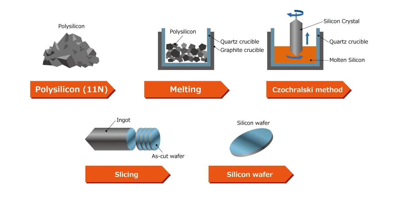
The representative crystal growth method is the Czochralski process. In this method, polycrystalline silicon is melted at approximately 1420°C in a quartz crucible, and a small single-crystal silicon piece (seed crystal) is brought into contact with the molten surface. Subsequently, the seed crystal is slowly pulled upward while simultaneously rotated, allowing crystal growth at the interface with the melt.
By precisely controlling the pulling speed, rotation rate and temperature distribution, the diameter and crystal quality are stabilized, ultimately forming a cylindrical single-crystal ingot that can exceed 300mm in diameter.
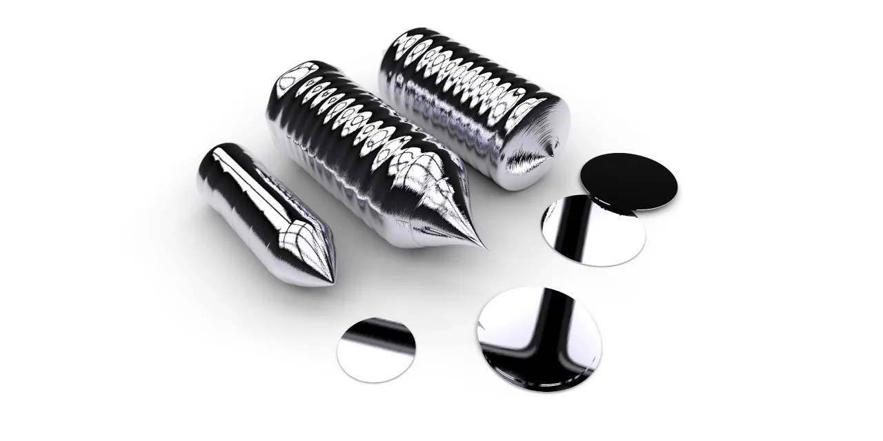
The grown silicon single-crystal ingot undergoes precision processing (outer diameter grinding) to match standard dimensions, typically finishing to a standard size of 300mm (12 inches) in diameter.
It is then sliced into disk shapes just a few hundred microns thick using ultra-fine diamond wire saws. This becomes the prototype of a silicon wafer.
The wafer surface immediately after slicing retains cutting marks, thickness variations and microscopic damage layers, making it unusable for semiconductor manufacturing as-is. Grinding and lapping flatten the surface, which is then finished to atomic-level smoothness through chemical mechanical polishing (CMP).
Furthermore, cleaning processes using ultrapure water and chemical agents completely remove particulates, metallic contamination, and organic residues.
The mirror-finished wafer completed in this way becomes a blank canvas for forming the fine circuits of semiconductor devices.
The disk shape of wafers is not only due to the cylindrical shape of ingots but also because it is most advantageous for ensuring physical uniformity throughout the manufacturing process. In processes such as polishing, film deposition, photolithography and etching, where wafers are rotated for treatment, circular substrates can maintain more uniform film thickness distribution and exposure amounts. Compared to substrates with corners, stress concentration is reduced, lowering the risk of chipping and cracking.
Thus, the disk-shaped silicon wafer is not merely a convention, but an optimal shape supported by the physical rationality of semiconductor processes.
Not Just Silicon: Diverse Compound Semiconductors Supporting Modern Society
While silicon has established an overwhelming position as a material supporting the semiconductor industry, it is not perfect for all applications. To achieve functions such as specific high-frequency operation, high-temperature environments, high-efficiency operation under strong electric fields or light emission and detection, silicon alone faces physical limitations.
This is where compound semiconductors, created by combining multiple elements, come into play.
Various compound semiconductors have been developed and commercialized according to applications, demonstrating excellent characteristics that silicon lacks.
Let's examine representative compound semiconductors, their raw materials, characteristics and areas of application.
Gallium Arsenide
Gallium arsenide (GaAs: a compound of gallium = Ga and arsenic = As) is a representative III-V compound semiconductor composed of Group III and Group V elements.
Compared to silicon, it has higher electron mobility (approximately 8500 cm²/V·s) and faster electron saturation velocity, characterized by less carrier scattering even during high-frequency operation.
It is optimal for low-noise, high-speed signal processing and high-frequency devices, enabling stable operation even in frequency ranges above several tens of GHz, which are difficult to achieve with silicon.
GaAs devices are widely adopted in high-frequency analog circuits such as 5G communication modules in smartphones, Wi-Fi transceivers and satellite communication equipment.
Unlike silicon, GaAs is a direct bandgap semiconductor with the property of efficiently emitting
light.
Leveraging this characteristic, it plays an important role in optoelectronics fields such as
laser diodes, light-emitting elements for optical communications, and infrared detectors.
In particular, vertical-cavity surface-emitting lasers used in smartphone facial recognition systems and high-speed lasers for optical fiber communications are based on GaAs materials.
Thus, GaAs serves as a bridging semiconductor for both high-speed electronic devices and optical devices, supporting modern communication and sensing technologies.
Gallium Nitride
Gallium nitride (GaN: a compound of gallium = Ga and nitrogen = N) is widely known as a light-emitting material for blue light-emitting diodes (LEDs), but in recent years it has rapidly gained attention in the power semiconductor field.
GaN has high hardness and a mechanically and chemically stable crystal structure and is classified as a direct bandgap wide-bandgap semiconductor (approximately 3.4 eV).
Its characteristics include a breakdown electric field approximately 10 times higher than silicon, suppressing leakage current even under high voltage application.
Additionally, carrier drift velocity is fast and switching operation losses are low, enabling high-frequency, high-efficiency operation.
With high thermal conductivity and stable performance even in high-temperature environments, it is considered an optimal material for electronic devices requiring energy savings and miniaturization.
In practical applications, adopting GaN transistors in power conversion circuits for smartphone fast chargers has enabled smaller, higher-output products compared to conventional silicon devices.
Applications are expanding as core technology for high-efficiency power systems, including data center power supplies, communication base stations, 5G infrastructure equipment and even onboard chargers and DC-DC converters for electric vehicles (EVs).
Silicon Carbide
Silicon carbide (SiC) is a group IV compound semiconductor composed of silicon (Si) and carbon (C). Crystal structures include multiple polytypes such as 4H-SiC, 6H-SiC and 3C-SiC, each with slightly different electron mobility and bandgap widths, but all commonly possess very high breakdown electric fields, high-temperature operating performance, and low power loss.
Even in high-voltage regions of several hundred volts or more, where silicon devices become difficult to control, SiC power devices can handle voltages in the thousands of volts range and large currents.
Low switching losses result in high energy efficiency and the advantage of suppressing heat generation.
Due to these characteristics, SiC is rapidly spreading as a core material supporting next-generation power electronics.
Adoption is particularly advancing in fields requiring energy conservation and high reliability,
such as inverters for EVs and hybrid electric vehicles, power converters for solar and wind
power generation, high-speed railway vehicles and industrial motor control systems.
In practice, since commercialization in the late 2010s, SiC power devices have rapidly expanded,
centered on the EV market, triggering large-scale mass production investment competition across
the industry.
Inverters using SiC have dramatically increased energy conversion efficiency. For example, full SiC inverters adopted for the first time in Japanese railway vehicles have reported power reduction of approximately 40% compared to conventional systems. With reduced cooling requirements enabling miniaturization and weight reduction, they also contribute to extending EV driving range and shortening charging time.
Diversifying Compound Semiconductor Materials and Their Challenges
Beyond the materials introduced so far, various compound semiconductors are being developed according to applications.
For example, indium gallium nitride (InGaN) is widely used as the primary material for blue and green LEDs, with GaN or InGaN-based materials playing central roles in blue LEDs. InGaN can control emission wavelength by adjusting indium (In) content, making it a core material in optoelectronics fields such as full-color LEDs, white lighting and high-brightness displays.
Additionally, gallium oxide (Ga₂O₃) is attracting attention as a next-generation ultra-high-voltage power semiconductor candidate.
Theoretically, it possesses a critical electric field strength (approximately 8 MV/cm) about twice that of SiC, with expectations for achieving both higher voltage and higher efficiency in devices.
Because it uses oxides as raw materials, material costs are relatively low, with potential for more affordable supply than SiC or GaN. Currently in the research and development stage for crystal growth and device technology, the ability to partially repurpose existing Si or SiC manufacturing equipment is also known as an advantage, with potential to become a new-generation power device material combining high performance and low cost in the future.
Compound semiconductors also present several challenges. Representative issues include difficulty in increasing crystal diameter compared to silicon (smaller wafer sizes), higher occurrence rates of crystal defects accompanied by brittleness and high raw material and process costs.
However, because they can achieve high-frequency characteristics, high-voltage withstand capability and light-emitting functions unattainable with silicon, they are expected to play increasingly important roles in cutting-edge fields such as 5G communications, renewable energy, automotive power control and optical sensing.
Semiconductor Raw Material Quality Determines the Future
Semiconductor chip performance depends not only on circuit design and microfabrication technology but heavily on the quality of raw materials used. In the atomic-level precision world, impurities and crystal defects in materials directly affect device reliability and yield.
Commitment to Purity
In the semiconductor industry, the question of how to prepare silicon with minimal impurities in a defect-free crystal structure has always been the greatest challenge and driving force for evolution.
Since even impurity contamination at the parts per million level affects device characteristics,
material manufacturers compete in pursuing high-purity technologies that challenge the
limits.
For polysilicon, the raw material for silicon wafers, purity of 99.999999999%, or 11N is already
standard level, and research targeting regions with 13 or 15 nines after the decimal point
(13N-15N) has advanced in recent years. Achieving such high purity requires not only precise
chemical refining processes but molecular-level control technologies including environmental
management during processes, material selection for reaction equipment and cleanliness
maintenance of gas supply systems.
Crystal growth technology that detects and suppresses dislocations and microdefects slightly contained in silicon crystals is also essential.
Non-uniform structures in crystals lead to device yield and electrical characteristic variations, so in recent years, non-destructive evaluation technologies using X-ray topography and infrared scattering methods have developed.
By eliminating impurities and structural defects to the limit, approaching intrinsic semiconductors, higher-speed, higher-performance, higher-reliability transistors and memory can be stably mass-produced.
This invisible material purity competition is truly the behind-the-scenes protagonist fundamentally supporting semiconductor chip performance improvement.
Supply Chain Importance
Stable raw material supply is also indispensable for the semiconductor industry.
Looking at the silicon raw material supply chain, Japan's domestic production of metallurgical-grade silicon, the stage before polycrystalline silicon, ceased in the 1980s, and currently all is imported from China, Norway, the United States and other countries.
On the other hand, Japanese companies account for approximately 60% of the global silicon wafer
manufacturing market, with high concentration in specific companies and regions.
This is two sides of the same coin with supply chain risk—for example, if major supply sources
stop due to large-scale disasters or changes in international circumstances, impacts could
spread throughout semiconductor production.
Indeed, geopolitical risks surrounding semiconductor materials have materialized in recent years.
In 2023, the Chinese government announced regulatory measures for exports of gallium and germanium, rare metals essential for semiconductors, with substantive export restrictions through a licensing system beginning in August.
Since China accounts for most of the world's gallium production, which is a raw material for GaAs and GaN, movements for alternative procurement and inventory securing is emerging in various countries.
With resource securing and supply networks potentially becoming political cards, supply chain strategies for raw materials are being emphasized more than ever in the semiconductor industry.
Summary
The semiconductors that power our smartphones, PCs and automobiles appear to be crystals of cutting-edge high technology.
However, their origins lie in materials such as sand (silicon dioxide) existing around us and compounds combining multiple elements.
These raw materials undergo extremely advanced refining and crystal growth technologies to be purified and controlled to the atomic level, transforming into semiconductor substrates capable of forming nanometer-scale precision circuits.
With the advancement of next-generation technologies such as AI, 5G communications, autonomous driving and IoT, semiconductors require even greater high performance and high efficiency than ever before.
In response, evolution toward greater purity and greater functionality in both materials science and manufacturing technology is indispensable for sustainable development of the semiconductor industry.
The world of raw materials, usually invisible, is the foundation that determines the future of semiconductors.
Silicon purity, compound diversity and the technological innovations supporting them are the driving forces building the next technology era.
Rapidus collaborates with world-class material manufacturers, constructing a manufacturing system with quality as its top priority.
- #Semiconductor
- #Silicon
- #Wafer
- #AI
- #Transistor
Recommendation