Technology
Rapidus' Vision: 100% Single-Wafer Processing for Next-Generation Chip Manufacturing
Semiconductors are essential parts used in everyday devices like smartphones, computers and cars. Producing them involves many steps, mainly divided into two stages: front-end processing and back-end processing. In this article we will discuss how single-wafer processes are advancing semiconductor manufacturing.
Semiconductor Manufacturing: Front-End and Back-End Processing
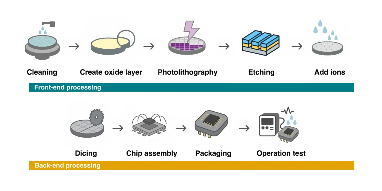
In front-end processing, tiny circuits like transistors and wires are created on a thin, round slice of silicon called a wafer. A silicon wafer is made by cutting a large crystal of silicon, called an ingot, into thin disks. The bigger the wafer, the more chips you can make at once. That's why modern chip factories use large wafers that are 300mm (about 12 inches) wide, and the equipment inside is designed to handle them.
The chip-making process involves many steps, starting from washing the wafer and then creating an oxide layer, drawing patterns with photolithography (with resist coating, exposure and development); etching away parts; adding ions; creating metal and insulating layers; and smoothing surfaces. These steps are repeated many times to build complex layers of circuits. In front-end processing, these steps are repeated on the same wafer to build the parts and connections that make up an integrated circuit (IC).
In back-end processing, after building the circuits, the wafer is cut into individual chips, called dies. These chips are then mounted on package substrates and equipped with external leads so they can function in electronic devices as a semiconductor. This part includes cutting the chips known as dicing; attaching them to substrates with die and wire bonding or bump joining; sealing them with protective molding resin materials; and conducting electrical testing to ensure they work correctly.
Typically, the back-end processing is done by outsourced semiconductor assembly and test (OSAT) companies, while the front-end is handled by entities known as foundries. So, in today's semiconductor industry, the designing, building and packaging of chips are usually done by many specialized companies at different locations. Recently, there has been a growing need to pair powerful processors, such as those used in AI, especially CPUs and GPUs, with fast memory to handle large amounts of data quickly. This involves connecting or stacking completed chips within a package to enable high-bandwidth, short-distance communication to satisfy performance and power requirements—a method known as chiplet integration.
Single- vs. Batch-Wafer Processing: What's the Difference?
In front-end processing, there are two types of equipment to process wafers: one is called a single-wafer process, where wafers are handled one by one, and the other is a batch process, where many wafers are processed all at once
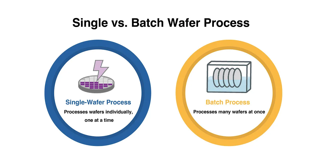
Single-Wafer Process: One Wafer at a Time
In a single-wafer process, each silicon wafer is handled one by one. This allows for very precise control, so the process is highly accurate and consistent. It's especially useful when making advanced chips that need fine detail and high performance, such as high-resolution complementary metal-oxide-semiconductor (CMOS) image sensors and advanced CPUs. This method is often used in producing semiconductors for smartphones, AI and self-driving cars, where delicate and careful processing is needed.
One major advantage of this method is that it helps keep differences between wafers small, which makes it easier to get more working chips from each batch. The machines used in this process can also collect detailed data during processing, for example, using sensors, which makes it well-suited for AI-based control and feedback to improve the process in real time.
On the other hand, because this method processes wafers one by one, it takes more time compared to a batch process, and it is not ideal for making large numbers of chips quickly. The machines are also more expensive due to the high level of control required, and more units may be needed. For these reasons, it usually costs more when making chips in high volumes.
Batch Process: Many Wafers at a Time
In a batch process, many wafers, sometimes dozens, are placed together in a chemical bath or heating furnace and processed all at once. This processing method is highly efficient and keeps costs down, which makes it great for producing a large number of chips. It is often used for products that need to be made in large quantities, such as memory chips and standard logic circuits.
Because many wafers are processed at once, the cost per chip goes down, and the equipment cost can be shared across more wafers. A batch process is a well-established and reliable method that has been used for a long time.
But one downside is that processing so many wafers at the same time can cause slight differences in process conditions between them, which may affect quality. Additionally, because this method processes everything in bulk, it is more difficult to adjust settings or fine-tune changes, making it less suitable for small-lot production or frequent process changes. Further, depending on the step, swapping wafers or heating and cooling them can take a long time.
| Item | Single-Wafer Process | Batch Process |
|---|---|---|
| Processing Method | Processes wafers individually, one at a time | Processes many wafers at once |
| Efficiency | Low (because wafers are processed one by one) | Very high (because many wafers are processed together, saving time) |
| Cost per Chip | More expensive (equipment and operation cost more) | Cheaper (cost is shared across many wafers) |
| Quality & Uniformity | Highly precise and consistent (each wafer gets precise control) | Less consistent (differences can happen between wafers) |
| Best Applications | For advanced chips and products that need fine details and high performance | For producing large amounts of basic chips (such as memory or logic chips) |
| Flexibility (Changing Conditions) | High (easy to adjust conditions for different products) | Low (hard to change settings or handle small batches) |
Why Single-Wafer Processes are Getting More Popular
Recently, more factories are switching to single-wafer processes. This shift is happening for two main reasons: advances in technology and changing market needs.
On the technical side, today's semiconductors are getting smaller, with finer linewidths and more complex 3D structures. This means the margin for error in process conditions has become extremely small. Therefore, it is more important than ever to control the process very carefully and precisely, and to make sure each wafer is treated uniformly - something single-wafer processes excel at. In fact, since fabs started using 300mm wafers, many steps like cleaning and annealing have been shifting from batch processes to single-wafer processes. For example, cleaning used to mean soaking lots of wafers in a chemical bath, but since the move to 300mm wafers, factories have increasingly introduced machines that clean wafers one by one using a chemical spray for better precision.
At the same time, the semiconductor market is changing. Instead of producing large amounts of a single, general-purpose chip, there are growing trends for quickly producing custom chips for different uses. Single-wafer process systems make it easier to change settings and switch between small and large production runs. That's why many chip-making foundries are adding more of these machines to handle both small test runs and large-scale manufacturing efficiently.
An Important Rapidus Goal: Enabling a Fully Single-Wafer Process Line
One of the key technical goals of Rapidus is to build a semiconductor production line that uses only single-wafer processes in its front-end. Instead of processing wafers in bulk as was common in the past (usually 25 at a time), Rapidus will focus on processing wafers one by one, every time, in every machine.
This is a big challenge because even steps such as heating (oxidation, diffusion or annealing) and cleaning, which are still often done in batches, will all be done one wafer at a time.
Modern chip-making involves hundreds of process steps. Building chips at the 2nm technology level can take years to go from design to finished product.
By utilizing only single-wafer processes in its operations, Rapidus can collect and analyze huge amounts of data from each wafer. This will help improve quality and yield, while also providing useful feedback to improve chip design. This approach is part of a bigger idea called Manufacturing for Design (MFD), which means using manufacturing data to support better design. As a result, it can also help shorten the time it takes to go from design to a working chip.
Another benefit of this system is its flexibility in producing a wide variety of custom chips. In addition to mass-producing general chips, Rapidus will also manufacture special custom chips for customers with different needs. To achieve this, production line flexibility is key. By starting from scratch and building an advanced production line, Rapidus' new Innovative Integration for Manufacturing (IIM) foundry will be optimized for single-wafer processes, full automation and smart sensors, making it one of the fastest and most sophisticated fabs in existence.
This flexible, high-precision setup based on single-wafer processes is central to Rapidus' new business model. Under the concept of its Rapid and Unified Manufacturing Service (RUMS), Rapidus will handle everything from front-end to back-end of chip-making, closely tied to the chip design process.
A wafer is a thin, round piece of material used as the base for making semiconductors. It is usually made of silicon. Tiny circuits and transistors are built on top of the wafer, and it eventually becomes a computer chip or processor.
RUMS stands for Rapid and Unified Manufacturing Service. It refers to the business model that Rapidus is developing. The concept is to handle everything from chip design to manufacturing, within a unified system, so they can quickly produce and deliver high-tech custom chips and chiplets using the latest 2nm Gate-All-Around (GAA) process technology.
- #Semiconductor
- #Front-End
- #Single-Wafer Process
- #Wafer
Recommendation