People
The Reality of IIM-1: Manufacturing the World's Most Advanced 2nm Semiconductors — The Vision Behind the "Soul Lot"
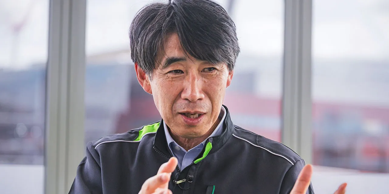
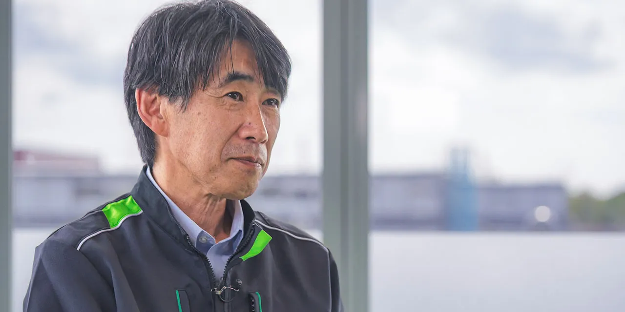
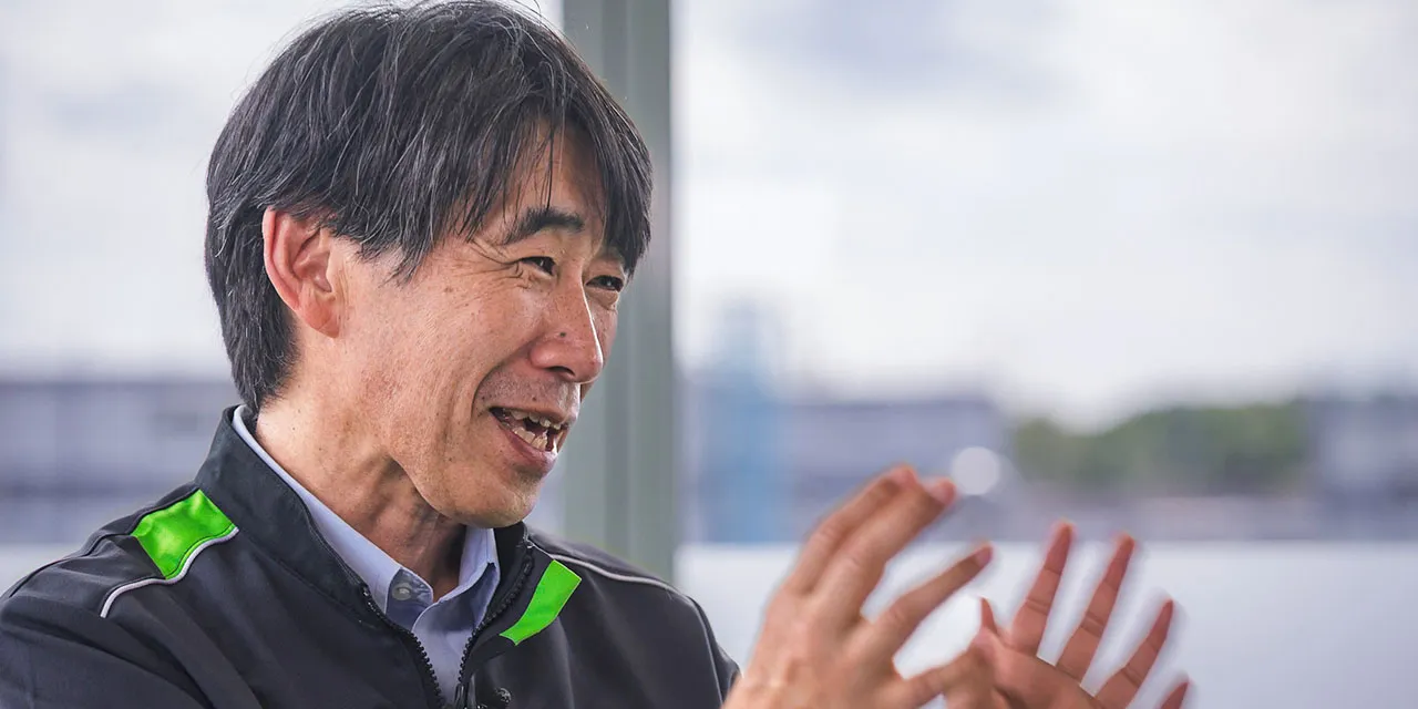
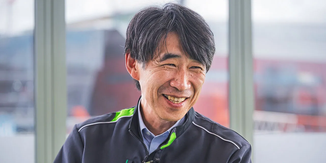
Atsuo Shimizu
Representative Director, Senior Managing Executive Officer, Head of Operations Division
Key Points of This Interview
- At IIM-1, Rapidus rapidly launched a 2nm pilot line and confirmed operation of GAA transistors.
- The “Soul Lot” united hundreds of engineers in a zero-to-one challenge toward mass production.
- Through EUV, shortest TAT and sustainable manufacturing, Rapidus is building the future of advanced semiconductors.
On July 18, 2025, Rapidus announced the successful operation of its gate-all-around (GAA)
transistors for the world's most advanced 2nm semiconductors.
Only a few people have
an inside look at our recent achievements at our Innovative Integration for Manufacturing
(IIM-1) foundry in Chitose City, Hokkaido, where the pilot line is being operated. We spoke with
Atsuo Shimizu, representative director, senior managing executive officer and head of operations
to learn about the exciting onsite milestones.
The Vision, Construction of IIM and Milestones Leading to the Pilot-Line Launch
―― You've progressed at lightning speed development to confirm the operation of GAA transistors. Can you tell us about the journey from the company's establishment to this point?

What stands out in the construction of IIM-1 is the groundbreaking ceremony held on September 1, 2023. After that, IIM-1's exterior rapidly took shape, and since then, we've been running at full speed. Last December, we took delivery of and installed the EUV lithography tool from ASML that performs circuit-pattern exposure.
We've achieved our milestones on time so far, but because challenges keep emerging one after another, there's never been a moment to catch our breath. This situation of clearing and navigating obstacles will not change, but we continue to meet and overcome new challenges head on as one team.
―― Can you tell us about what's currently going on inside IIM-1?
After bringing in the EUV lithography machine, we installed and started up more than 200 semiconductor tools that were required to construct the pilot line and begin prototyping. We showcased the completed prototypes to customers and other stakeholders at the customer event held in July 2025.
Being able to produce prototypes at incredible speed—and to confirm their operation—was a major step forward.
Simply installing and connecting tools does not mean we can start production. We need cooperation from equipment manufacturers for process applications, including recipes and software, tuning and other adjustments. Additionally, while we received the technology transfer from IBM, we are tackling challenges on our own every day—wrestling with questions like "How can we meet our targets?" to improve characteristics, such as performance, toward mass production.
The Engineers' Journey Through Prototype Production
―― How did the people on the ground succeed in producing the prototypes and how do they feel about their work now?

Our CEO, Dr. Atsuyoshi Koike, called the very first prototype the Soul Lot. Until the Soul Lot was completed, the approximately 400 engineers working at IIM-1 and employees at our headquarters—about 600 people in total—were watching over it. Everyone treated the on-time, extremely fast-flowing process as their own priority, carefully keeping an eye on the outcome of this critical milestone.
Having hundreds of people focused on a single lot like that is rare.
In a typical semiconductor fab, you would run a lot with the factory already completed and production equipment in place.
However, for us, everything—the building, the tools and resources including people—was a launch from zero. That is why everyone could focus on the Soul Lot and showcase our strength as a team.
Currently, we're advancing multiple prototypes.
Key Technologies for Mass Production of World-Leading 2nm Semiconductors and Achieving Shortest Turnaround Time (TAT)
―― Mass production of 2nm semiconductors—and achieving shortest TAT—requires various tools, including EUV lithography. Could you tell us about the key tools?

Currently, ASML in the Netherlands is the only company that can manufacture EUV lithography tools. We were the first in Japan to introduce this as a mass-production tool.
However, if we simply accepted ASML's requirements as-is, it would have required us having our cleanroom ready several months before installation. For a typical fab with existing facilities, this wouldn't be a problem, but we had to advance pre-construction for the EUV tool while simultaneously constructing the factory.
So, we decided to break down the requirements and examine them one by one. For example, there were conditions for temperature, humidity, cleanliness, etc., that needed to be addressed where the new machine would be installed. Through persistent negotiations with ASML and advancing construction and pre-construction at incredible speed, we successfully took delivery in December 2024.
Meanwhile, to achieve shortest TAT, we introduced a new transport system, that represents a first for the foundry industry. We installed a ceiling-mounted transport equipment in parallel with construction. At the time, there were debates about whether it could really be completed, in addition to using a little bit of imagination of how it would operate after completion, but I am very proud to say, it is now running smoothly.
―― We've heard you're putting considerable effort into environmental measures. Why such emphasis?
Koike-san constantly says that the semiconductor industry must be sustainable. As long as humanity seeks further technological advancement, densification and higher performance, advanced semiconductors will continue to be demanded.
Since the Industrial Revolution—especially in the last 40 years—we have used a lot of energy and chemicals.
However, energy may eventually be depleted, or chemical regulations may become stricter, potentially prohibiting certain materials or processes. If that happens, semiconductor manufacturers worldwide won't be able to keep up with technological progress.
To avoid that, we must continue operating our business without burdening the environment or accelerating any environmental damage. That has been in Koike-san's mind since we decided to operate in Chitose.
Therefore, it's vital to consider CO₂ emissions.
Currently, there are no supplier factories in Hokkaido, so materials are transported from Honshu (the main island of Japan). If suppliers transport individually, CO₂ emissions increase, so we are implementing a centralized delivery process by collecting materials at specific points.
Current Thoughts and Future Prospects
―― Can you tell us what steps you'll take toward mass production?
As we advance toward starting mass production in 2027, we face a variety of challenges and opportunities including yield improvement and reliability enhancement. Addressing yield improvement and reliability is essential for products manufactured by Rapidus as they will be installed in various devices, including servers, and will be required to deliver maximum performance.
More specifically, our goal is to enable customers to establish Rapidus foundry feasibility for their own product designs using our process design kit (PDK) that we will provide to early customers. The PDK will include Rapidus AI-Agentic Design Solution (Raads), the semiconductor development tool we are building and data showing the performance of the advanced semiconductors we will manufacture. Customers will use this information to determine whether their product designs are the right fit for our foundry.
―― Let me also ask about back-end processes. Can you tell us about the future development of Rapidus Chiplet Solutions (RCS), which is currently being constructed?
Currently, within Seiko Epson's Chitose facility adjacent to IIM-1, we are advancing equipment installation, tool start-up and cleanroom construction to establish RCS, our back-end pilot line. Advanced packages manufactured in back-end processes include multiple technologies such as chiplets and 3D packages, and we are preparing to support all of them. We will start developing these technologies in 2026, with the goal of constructing a back-end line at IIM-1 starting in 2027.
The World Rapidus Aims For
―― What kind of presence does Rapidus want to provide to customers?

There are only a few companies in the world, including ours, working on advanced 2nm semiconductor process development.
We will leverage our strength in the shortest TAT and work hard to be recognized by more customers as one of their leading foundry options.
Today, it's taken for granted that airplanes fly through the sky. Though once thought impossible, humans have continued to evolve. As long as human aspirations persist, the need for advanced semiconductors will not disappear. Technological progress has never stopped.
As long as technological advancement is demanded, engineers will never give up. Today's interview paused when we heard airplanes overhead, but someday, completely silent airplanes might be developed.
Even when we become mass-production-ready for advanced semiconductors, we will not stop. We will continue to innovate for our customers.
- ※1 Turnaround time (TAT): The time from when a product enters the line and starts flowing until it's completed. Achieving short turnaround time also requires reducing time not directly involved in production, such as transport.
- ※2 Process Design Kit (PDK): A collection of design information and tools necessary for circuit design in semiconductor processes.
- ※3 Rapidus AI-Agentic Design Solution (Raads): A semiconductor design support service from Rapidus utilizing AI/ML, aiming to shorten design cycle time and significantly reduce costs.
- ※4 Chiplet: A technology that builds large-scale systems by combining multiple semiconductors with different functions within a single package. There are types that combine multiple logic semiconductors while others that include logic and memory in one package.
- ※5 3D package: A packaging technology that stacks multiple semiconductors vertically. The semiconductors are electrically connected through vertically installed through-silicon vias (TSVs).
- #Interview
- #Atsuo Shimizu
- #IIM
- #Raads
Recommendation